Photonic band-gap (PBG) structures were initially proposed in the optical component field. In the microwave field, PBG periodic structures suppress the propagation of electromagnetic waves whose frequencies are within certain bands. They allow shifting the rejected frequency band by simply changing the geometry parameters of the PBG element or the physical characteristics of the PBG structure.
In recent years, because of these special properties, PBG structures have been widely used in the control of propagation of electromagnetic waves.
In the past few years, much research has been done in one- or two-dimensional PBG structures.1–9 Most of the PBG structure elements are formed by simple geometries, such as a circle or a rectangle.
4,5 Because PBG structures are periodic, most of them will generate periodic band-gaps from higher order modes. Although the bandwidth of the main band-gap can be increased, the main band-gap is often not wide enough and the required bandwidth cannot be extended.
This is due to an appreciable distance between the center frequencies of the periodic band-gaps. The relative bandwidth of the stopband can usually reach 30 percent.
1,7 In this article, a new photonic band-gap structure for microstrip lines is proposed.
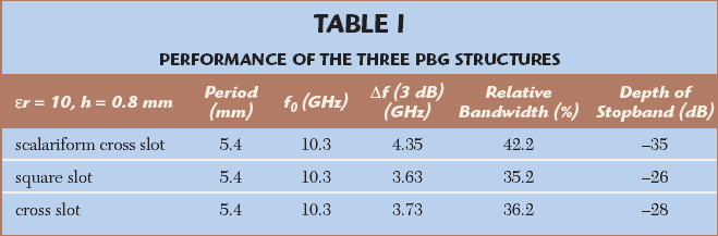
The periodic 2-D patterns, consisting of slots in the shape of crosses with squares in the middle (scalariform) etched in the ground plane of microstrip lines, can effectively increase the bandwidth of the stopband. The relative bandwidth can reach 40 to 50 percent.
The proposed slot structure can easily be designed and fabricated using conventional printed circuit board technology.
PBG Structure Design
As is well known, if the period of the PBG elements is chosen to be half the guided wavelength at the center frequency of the stopband, the electromagnetic band-gap structure produces a stopband in which propagation is suppressed. The PBG structure is implemented by etching slots in the ground plane, as shown in Figure 1.
The dielectric constant of the substrate is ?r = 10 and its thickness is h = 0.8 mm. The length of every side of the cross-slot is kept constant and equal to 0.9 mm; the period is 5.4 mm. The microstrip line width is 1 mm for Z0 = 50 ?. The circuit simulation was performed using HFSS.
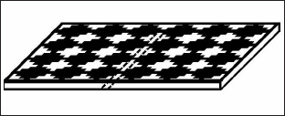
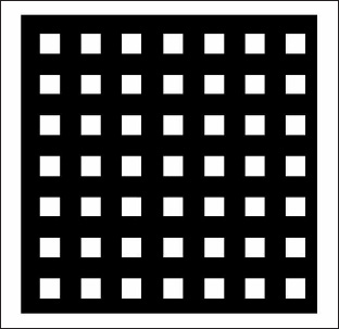
To make a comparison, other structures composed of simple geometry patterns such as squares and crosses are also simulated, as shown in Figures 2 and 3. All these PBG structures are composed of patterns of 7 × 7 elements.
In general, the stopband center frequency f0 is a function of the period of the structure. The three structures are all based on the same substrates and have the same period. Consequently, in all three cases, the center frequency of the stopband is approximately 10 GHz.
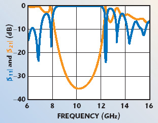
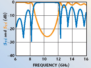
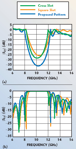
The magnitude and bandwidth of the stopband, however, depend on the geometry of the PBG pattern. The simulated performances for the three patterns are shown in Figures 4, 5 and 6. The comparative data is listed in Table 1.
It can be easily observed from the simulated results that the performance of the PBG structure with the proposed scalariform pattern is much better than that of the PBG structures with square and cross patterns.
Experiment and Measurements
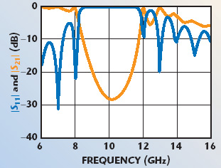
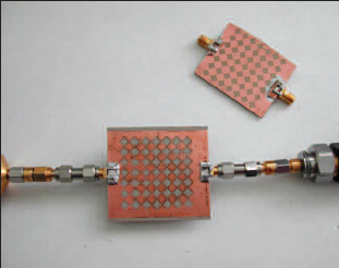
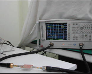
Experiments were performed to demonstrate the suppression of the propagation of electromagnetic waves. A fabricated PBG sample, with a pattern arrangement of 7 × 7 elements, is shown in Figure 7. Figure 8 shows the experimental setup used for the measurements. The two ends of the microstrip line are soldered to two SMA connectors.
The results are shown in Figure 9. The PBG sample with the proposed pattern has a rather wide bandwidth characteristic. The central frequency of the stopband is 10.5 GHz; the bandwidth is about 5 GHz. In the stopband, the rejection level can reach –47 dB. Outside the stopband, the return loss of the microstrip line is less than 1.5 dB. The measurement results agree well with the simulation results.
Conclusion
A novel microstrip line with a scalariform (cross plus square) slot PBG structure has been proposed. The new PBG structure can effectively increase the width of the stopband compared with some other PBG structures composed of simple geometry slots. Both the simulated and experiment results have shown that a wide stopband is achieved for this PBG structure.
References
1. V. Radisic, Y. Qian, R. Coccioli and T. Itoh, “Novel 2-D Photonic Band-gap Structure for Microstrip Lines,” IEEE Microwave and Guided Wave Letters, Vol. 8, No. 2, February 1998, pp. 69–71.
2. H. Rong, X.X. Zhang and G.B. Xin, “2-D PBG Structure in Microstrip Line and Symmetrical Microstrip Line,” 2000 Asia-Pacific Microwave Conference Digest.
3. T.Y. Yun and K. Chang, “One-dimensional Photonic Band-gap Resonators and Varactor Tuned Resonators,” 1999 IEEE International Microwave Symposium Digest, Vol. 4, pp. 1629–1632.
4. D. Dawn, Y. Ohashi and T. Shimura, “A Novel Electromagnetic Band-gap Metal Plate for Parallel Plate Mode Suppression in Shielded Structures,” IEEE Microwave and Wireless Components Letters, Vol. 12, No. 5, May 2002, pp. 166–168.
5. J.S. Sun and G.Y. Chen, “Microstrip Line with the PBG Structures,” Proceedings of the APMC2001, Taipei, Taiwan, ROC.
6. H. Liu, Z. Li and X. Sun. “Compact Defected Ground Structure in Microstrip Technology,” Electronics Letters, Vol. 41, No. 3, 2005.
7. J.M. Hickmann, D. Solli, C.F. McCormick, R. Plambeck and R.Y. Chiao, “Microwave Measurements of the Photonic Band-gap in a Two-dimensional Photonic Crystal Slab,” Journal of Applied Physics, Vol. 92, No. 11, 2002.
8. F. Yun-qi, Z. Guo-hua and Y. Nai-chang, “A PBG Microstrip Line with Fractal Characteristics,” ACTA Electronic Sinica, 2002.
9. V. Radisic, Y. Qian, R. Coccioli and T. Itoh, “Novel 2-D Photonic Band-gap Microstrip Structures,” Microwave and Optical Technology Letters, Vol. 22, No. 9, 1999.