
Because of the rapid growth in density and complexity of modern integrated circuit interconnects, modeling has been a requirement in circuit design and simulations. On-chip interconnects have achieved a dominant role, especially in determining the performance of RF and monolitic microwave integrated circuits (MMIC). In the last two decades, the characterization of high frequency packages has become of considerable interest for MMIC applications.1,2 In spite of the production of many interconnect modeling tools based on certain techniques,3–8 a compact model for RF/microwave interconnects does not yet exist. Therefore, the development of a compact model for interconnects has become very important to achieve ‘design convergence.’
It is well known that at RF and microwave frequencies, to represent signal retardation, interconnects have been modeled by transmission lines. However, for high frequency analog RF and microwave circuit realization on one chip, a major problem is the physical implementation of interconnections that behave as transmission lines. It is therefore more convenient to model the interconnections as transmission lines, where the discontinuities and parasitics are modeled as lumped LC elements. For a more accurate electronic package, a typical single interconnect may be modeled with a transmission line of characteristic impedance Z0, terminated with shunt capacitors and serial inductors, as shown in Figure 1. Here, the package interconnection can be modeled by a transmission line Z0, the physical length of the line can be represented by the delay length t, the bonding wires and pads can be characterized by the serial inductances L1 and L2, and the shunt capacitances C1 for the die pad and C2b for the board pad, respectively.9

Fig. 1 A simple interconnect model.
In general, the interconnect models used for RF/microwave circuits can be characterized by transfer functions such as scattering parameters or lumped, distributed, mixed equivalent circuits representing the interconnects. In recent years, some studies have shown that in the design of RF/MMICs on-chip, the use of mixed, lumped-distributed elements instead of solely lumped or distributed elements is much more practical for physical realization.10–13 Therefore, in this work, mixed, lumped-distributed equivalent circuits are used to describe, model and analyse interconnects, in terms of simple lumped and distributed elements, so that all the parameters are naturally embedded in the design configurations. By utilizing these lumped-distributed models to describe lossless RF/microwave interconnects, a novel approach is presented. Thus, the modeling of interconnects encountered in the design of lossless RF/microwave circuits on-chip becomes more practical.

Fig. 2 A more general and accurate interconnect model.
Scattering Matrix Description for the Interconnect Model with Mixed Elements
As shown in Figure 2, the lossless two-port is composed of lumped elements and uniform transmission lines connected in cascade, and can be used to model the more general and accurate RF/microwave interconnects. Thus, the problem of interconnect modeling is reduced to the design of cascaded two-port networks with mixed, lumped-distributed elements. The lossless two-port constructed with a cascade connection of low pass ladders isolated with commensurate transmission lines has been described by using the two-variable scattering approach.13
Utilizing the properties (2 and 3) given in Aksen and Yarman,13 and by removing the cascaded transmission lines and the high pass type lumped elements (floating capacitors/shunt inductors) and the lumped elements from the composite interconnect structure, the low pass lumped and distributed models obtained are represented with the scattering matrices SL(p) and SD(?), respectively, as

In a similar manner, with the cascaded transmission lines and the low pass elements (floating inductors/shunt capacitors) removed, one would obtain a typical high pass lumped model. Like the low pass counterpart, the high pass interconnect model is represented with a scattering matrix SH(p)
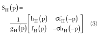
Where p denotes the complex frequency variable for the lumped models, ? is the Richard variable for the cascaded transmission lines, the hL(p), gL(p), hD(?), gD(?), hH(p), gH(p) polynomials are real, all {gL(p), gD(?), gH(p)} polynomials are strictly Hurwitz, fL(p) = ?, fH(p) = pk, fD(?) = (?–l2)n?/2 (here, k and n? denote the numbers of high pass type elements and unit elements, respectively).
Eventually, the interconnect network model with mixed elements given above can be described by means of a two-variable scattering matrix as
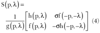
Where h(p,?), g(p,?) and f(p,?) are real polynomials of complex variables p and ?, f(p,?) is monic and contains the transmission zeros of the mixed structure. In a mixed structure constructed by a cascade connection of np lumped and n? distributed sections, the polynomial f(p,?) is defined by

? is a unimodular constant; |?|=1, g(p,?) is a scattering Hurwitz polynomial.
In another hand, the two-variable, real polynomials g = g(p,?) and h = h(p,?) can be expressed in coefficients form as
![]()
Where ?g and ?h area called as the coefficient matrices of the g(p,?) and h(p,?) polynomials as

The CAD Modeling Algorithm
The main goal of this algorithm is to construct the composite scattering matrix S(p,?), characterizing the mixed element interconnect structure by means of the polynomials hL(p), hH(p) and hD (?), using the following steps.
The Algorithm:
The inputs of this algorithm consist of the numbers of lumped and distributed elements in the mixed elements model and the independent coefficients used in describing the proposed interconnect networks together with the transmission zeros.
Inputs:
- nP and n?, the total numbers of lumped elements and commensurate transmission lines, respectively
- Coefficients of the hL(p), hH(p) and hD(?) polynomials, which represent the low pass lumped, the high pass lumped and the cascaded commensurate lines interconnect models, respectively
- k, the number of high pass type of elements with transmission zeros at origin in the p-domain
Step 1:
- Using the losslessness conditions of the models with one-kind of elements (the low pass type or the high pass type lumped elements, or only transmission lines), generate the equations into an even polynomial identity in p as follows:

- Find the roots of the polynomials GL(–p2), GH(–p2) and GD(–?2) obtained in Equation 7.
- Choose the LHP (left hand plane) zeros to form gL(p), gH(p) and gabD (?) polynomials as strictly Hurwitz.
Step 2:
- For the algebraic decomposition, select the degrees of both the lumped and distributed models.
- Apply the algebraic decomposition algorithm14 to decompose the lumped networks and the cascaded commensurate transmission lines into lower order subsections.
As a result of decomposition, the canonic scattering polynomials sets {gLi(p), hLi(p), fLi(p)}, {gHi(p), hHi(p), fHi(p)} and {gDi(?), hDi(?), fDi(?)}, which define the low pass (Equation 1), high pass (Equation 3) lumped and distributed (Equation 2) models, respectively, are obtained.
Step 3:
• Form the transfer scattering parameters for each subsection TLi(p), THi(p) and TDi(?).
• Multiply them in a desired order to end up with the transfer scattering matrix T(p,?) for the mixed model structure. As an example, the [LL1D1LH1D2........] order of the obtained simple subsections can be computed as
T(p,?)=TLi(p)Di?THi(p)TD2(?).......
In this step, the canonical polynomials h(p,?), g(p,?) and f(p,?) of the mixed structure in Equation 4 are obtained completely.
Step 4:
Selecting the coefficients of hL(p), hH(p) and hD(?) polynomials as free parameters of the mixed structure, optimize the transducer power gain of the composite interconnect model over the operating frequencies, given as

Where SG and SL are the reflections of the generator and the load networks.
Remark:
In order to model interconnects, one must obtain the measured data for the terminals so that the optimization algorithm is invoked for the modeling process.
Application
In this section, to validate the CAD method, two examples are considered. First, in a single-stage FET amplifier design, the front- and back-end interconnect circuits are modeled using the new CAD method. The second example deals with the modeling of a symmetric microstrip line. Both modeling examples are implemented on a computer by means of a MAT LAB™ toolbox, not generated as hardware. Thus, all the data obtained are only numerical optimization results, not actual measured results.
Example 1
By utilizing the CAD method proposed in this work, the source-to-active device and active device-to-load interconnects encountered in the design of a single-stage FET amplifier are modeled by mixed structures constructed with lumped and distributed components for 50? terminations. The measured scattering parameters for the amplifier active device (HFET2001) are given in Yarman and Carlin.15 In this example, two unit elements (UE) and three lumped elements are used for the input (front-end interconnect) and output (back-end interconnect) models, that is n? = 2 and np = 3.
In the above CAD procedure, fL(p) = 1, fH(p) = p for the input and fL(p) = 1, fH(p) = p2 for the output interconnect model are selected, which means that there will be one zero of transmission at p = 0 and two zeros of transmission at p = ? for the first, two zeros of transmission at p = 0 and one zero of transmission at p = ? for the second model, as given in Table 1.

Here, in order to end up with a transformer-free structure, hLFE0, hLBE0, hDFE0, hDBE0, hHFE1 and hHBE2 are set to zero. Using the above algorithm, the main goal of the design is to maximize the transducer power gain (TPG) given in Equation 8, over the normalized frequencies ?1 = 0.375 (6 GHz) to ?2 = 1 (16 GHz). Therefore, initializing the unknown model parameters (hLFE1, hLFE2, hLBE1, hHFE0, hHBE0, hHBE1, hDFE1, hDFE2, hDBE1, hDBE2), the TPG is optimized by means of the Levenberg Marquard LMS algorithm.

As the result of optimization, the following coefficients are obtained, describing the input and output interconnect networks as in Table 2. The final amplifier circuit and its performance characteristics are depicted in Figures 3 and 4, respectively.

Fig. 3 Final amplifier circuit.

Fig. 4 A Performance of the final ampliefier.
Fig. 5 The symmetric microstrip line prototype.
Example 2
As is commonly known, a microstrip line is normally used at the motherboard level on MMICs, due to its low loss. Thus, in Example 2, in order to get a more accurate microstrip line model as an interconnect structure, a symmetric microstrip line is modeled with mixed, lumped and unit elements by applying the method developed in this article. The canonic polynomial forms of the scattering parameters for the theoretical reference model of the microstrip line in Figure 5 are given in Table 3. In this example, the chosen reference model does not represent the real parameters of an actual microstrip line. However, this model is most appropriate for the interconnects encountered in practice, especially on MMIC.

In the example, four low pass type lumped elements and only one unit element, that is np = 4 and n? = 1 for the proposed model, are used. Applying the above CAD technique, the coefficients of the following h polynomials as free parameters in the optimization scheme are selected. Here, for a transformer-free structure, hL0 and hD0 are set to zero
![]()
The Model Parameters:

t(delay length of the unit element)
As the result of the numeric optimization, the coefficients describing the proposed model depicted in Figure 6 are obtained in Table 4; its performance characteristics are given in Figure 7.

Fig. 6 The proposed CAD model for the symmetric microstrip line.


Fig. 7 Performance characteristics of the microstrip line.
Here, the magnitude and phase of the input reflection function S11 are chosen as the objective function, Equation 9, employed by the least square error criteria in the optimization scheme.

Where {|SP| and ?(SP)} and {|S11| and ?(S11)} represent the magnitude and phase of the input reflection functions for the reference model and the CAD model, respectively. As seen clearly, a good agreement between the reference model and the proposed CAD model shows the validity of the method in the modeling of real RF/microwave interconnects.
Conclusion
In this article, a CAD procedure is presented for modeling interconnects with lumped and distributed components, based on combining the simplified real frequency technique with the Fettweis’s network decomposition algorithm. In the new method, the interconnect modeling networks are described by two-variable scattering parameters. Using any unconstraint routine in the optimization process, the free model parameters, initialized by ad-hoc choices (±1), are obtained easily.
This method provides a more general and accurate modeling of RF/microwave interconnects in terms of simple lumped elements and commensurable transmission lines. Also, the method makes the implementation of RF/microwave circuits practical by modeling the interconnects accurately such that the parasitic effects and discontinuities are naturally embedded in the design configurations.
The proposed CAD method is applied to a microwave amplifier design and a microstrip modeling, where lumped and distributed elements are used to model the parasitics and discontinuties in MMIC designs. However, the method can also be applicable to the modeling of high speed digital IC interconnects and electronic packages. It is hoped that this technique can be used in generating models as a CAD tool for complex interconnect networks.
References
1. R.A. Pucel, “Design Consideration for Monolitic Microwave Circuits,” IEEE Transactions on Microwave Theory and Techniques, Vol. 29, No. 6, June 1981, pp. 513–534.
2. Special Selection on Interconnects and Packaging, IEEE Transactions on Microwave Theory and Techniques, Vol. 42, No. 9, September 1994, Part 2.
3. C.L. Ratzlaff and N. Gopal, “RICE: Rapid Interconnect Circuit Evaluator,” Proceedings of the 29th ACM/IEEE Design Automation Conference, 1991, pp. 555–560.
4. M.M. Alaybeyi, J.Y. Lee and R.A. Rohrer, “Numerical Integration Algorithms and Asymptotic Waveform Evaluation (AWE),” IEEE International Conference on Computer-aided Design, 1992, p. 341.
5. D.D. Ling, S. Kim and J. White, “A Boundary-element Approach to Transient Simulation of Three-dimensional Integrated Circuit Interconnects,” Proceedings of the 29th ACM/IEEE Design Automation Conference, 1992, p. 93.
6. J.M. Jong, B. Janko and V.K. Tripathi, “Equivalent Circuit Modeling of Interconnects from Time Domain Measurements,” IEEE Transactions on Component, Packaging and Manufacturing Technology, 1993, pp. 119–126.
7. A. Odabas?oglu, M. Celik and L.T. Pileggi, “PRIMA: Passive Reduced-order Interconnect Macromodeling Algorithm,” IEEE Transactions on Computer-aided Design of Integrated Circuits and Systems, Vol. 17, No. 8, August 1998, pp. 645–654.
8. Q. Xu, Z.F. Li, P. Mazumder and J.F. Mao, “Time-domain Modeling of High Speed Interconnects by Modified Method of Characteristics,” IEEE Transactions on Microwave Theory and Techniques, Vol. 48, No. 2, February 2000, pp. 323–327.
9. TDA Systems Group, “TDR Techniques for Characterization and Modeling of Electronic Packaging,” HDI Magazine, April 2001.
10. B.S. Yarman and A. Aksen, “An Integrated Design Tool to Construct Lossless Matching Networks with Mixed Lumped and Distributed Elements for Matching Problems,” IEEE Transactions on Circuits and Systems, Vol. 39, 1992, pp. 713–723.
11. A. Sertbas, A. Aksen and B.S. Yarman, “Construction of Some Classes of Two-variable Lossless Ladder Networks with Simple Lumped Elements and Uniform Transmission Lines,” IEEE Asia-Pasific Conference Digest, Thailand, 1998, pp. 295–298.
12. A. Sertbas, A. Aksen and B.S. Yarman, “Construction of Analog RF Circuits with Lumped and Distributed Components for High Speed/High Frequency Mobile Communication MMICs,” ECCTD 1999, Stresa-Italy, Vol. 2, 29 August–2 September 1998, pp. 1123–1126.
13. A. Aksen and B.S. Yarman, “A Real Frequency Approach to Describe Lossless Two-ports Formed with Mixed Lumped and Distributed Elements,” International Journal of Electronic Communications, 2001, pp. 389–396.
14. A. Fettweis, “Factorization of Transfer Matrices of Lossless Two-ports,” IEEE Transactions on Circuit Theory, Vol. 17, 1970, pp. 86–94.
15. B.S. Yarman and H.J. Carlin, “A Simplified Real Frequency Technique Applied to Broadband Multistage Microwave Amplifiers,” IEEE Transactions on Microwave Theory and Techniques, Vol. 30, 1982, pp. 2216–2222.