
In wireless communications, linearization of the PA is sometimes required to ensure high quality of the modulated signal and maintain good PAE. PA linearization using a feed-forward technique1–4 can be very tedious and time consuming. Without PA linearization, an approach to achieve high power and good PAE is shown by using a class-AB PA device. Given an output power specification of 25 dBm, a PA device that has a P1dB 5 dB higher than the specification should be selected. A PA device with high P1dB is selected so that the device is matched for high output power at the beginning. After it is matched for power, the PA is operated at lower drain current. In this article, a commercial PA device (Fujitsu FLL177ME) was selected, which has a typical P1dB of 32.5 dBm. The PA design is accomplished based on the technique and small-signal S-parameter analysis demonstrated by Yeap, et al.5 The PA device is first matched for gain based on small-signal S-parameters provided by the manufacturer at 2.21 GHz, followed by passive load pull of the pre-matched amplifier using a slide screw tuner to achieve high output power. It is shown that the PA operating at lower drain current introduces minimum distortion to the modulated signal, based on the error vector magnitude (EVM) figure of merit measured. Although the output P1dB of the PA designed is slightly lower, the PAE and power gain remain excellent.
EVM Measurement of Medium Power Amplifiers
The EVM is the figure of merit widely used to justify the modulation accuracy. It is a measure of the constellation cluster variance due to any impairment or transmitter imperfections, measured relative to the ideal constellation point locations, as shown in Figure 1. The typical parameters used to analyse vector-modulated signals in an EVM measurement are RMS EVM, RMS magnitude error, RMS phase error, frequency error, I/Q offset and droop error per symbol. In this experiment, the impairment introduced by the PA is investigated, based on the measured numerical figures of RMS EVM (EVM) and RMS phase error (PE).

Fig. 1 Error vector magnitude and related quantities. 6
A vector signal generator (VSG) is used to generate digitally modulated signals and the EVM measurement is performed using an Agilent E4404B spectrum analyzer with the modulation analysis personally installed. The parameters set to generate a modulated signal source and to measure the demodulated signal are shown in Table 1. In this section, the EVM measurement of two medium power amplifiers are carried out on a WJ Communications WJAH102 gain block with a gain of 12 dB and P1dB of 25 dBm and on a Hittite HMC454ST89 HBT MMIC with a gain of 12.5 dB and P1dB of 27 dBm. Figure 2 shows the EVM measurement for modulated signals generated directly from the VSG to the spectrum analyzer, which serves as a reference. All measurements are taken for an average of 10 times. The modulated signal is then fed to the input of the amplifier under test (AUT) and the EVM measurement is performed at the output of the AUT. Figure 3 shows the output power measured using an HP power meter (EPM-441A) and the PAE for each AUT. Note that the output power measured with the modulated BPSK source is approximately 1 dB lower than for a continuous wave. Figure 4 shows the plot of EVM and PE against the test input power (Pin). The figures are plotted separately for clearer distinction of EVM, PE, PAE and output power with reference to the input power. It is shown that the AUT, operating near the P1dB region, distorts the modulated signal significantly.


Fig. 2 EVM measurement (reference).

Fig. 3 Output power and PAE versus input power at 2.1 GHz for (a) WJAH102 (PldB?25 dBm) and (b) HMC454ST89 (PldB?26.5 dBm) devices.

Fig. 4 EVM measurements on the amplifiers under test; (a) WJAH102 and (b) HMC4545T89.
Performance of PA Pre-matched for Power Gain
The EVM of the AUT shows that the EVM is less than 2 percent and the PE is less than 1°, when the amplifiers are operating at more than 4 dB down from the P1dB. In order to achieve a high PAE while minimizing the nonlinear distortion of a PA, the use of a PA device with a P1dB that is 5 dB higher than the actual output power requirement is proposed. In this article, a Fujitsu FLL177ME was selected, which has linear gain of 8.7 dB without impedance matching. Based on small-signal S-parameters given by the manufacturer, the PA device is first matched for power gain at 2.21 GHz by applying the conjugate impedance matching technique. The DC bias circuit is designed, based on the bias network proposed by Wei, et al.7 The PCB substrate used was Roger RO4003 having a thickness of 0.508 mm and relative permittivity ?r of 3.38. All PCBs were milled using the Quick Circuit System from T-Tech Inc. The PCBs are mounted on an aluminium plate for heat sinking and DC and RF grounds, as shown in Figure 5. The performance of the pre-matched PA is shown in Figure 6. Since the PA is only matched for gain, the P1dB is lower, leading to a greater measured EVM and PE, as the input power is increased.

Fig. 5 Circuit board of the pre-matched power amplifier

Fig. 6 Performance of the pre-matched power amplifier; (a) Pout and PAE and (b) EVM measurement.
Performance of PA Matched for Optimum Output Power
Following the design steps described by Yeap, et al.,5 a Maury Microwave slide screw tuner (model 2640D1) is cascaded after the pre-matched PA to locate the optimum load impedance of the PA. During load pull, the gate voltage can be varied accordingly to limit or lower the drain current and record the optimum load impedance at 2.21 GHz. Using small-signal S-parameter simulation in Agilent ADS2003, the output-matching network was optimized to match to the required load impedance measured. The layout is shown in Figure 7. With the optimized output-matching network, the overall performance of the PA improves significantly, as shown in Figure 8. The PA biased at Vgs = –1.4 V has a higher linear gain and output power than for Vgs = –2 V. However, the PA biased at Vgs = –2 V introduces less nonlinear distortion and has a higher PAE.

Fig. 7 Circuit board of the power amplifier matched for optimum load impedance.

Fig. 8 Performance of the optimized power amplifier at 2.21 GHz (a) Pout and PAE and (b) EVM and PE.
To validate the consistency of the PA performance based on such an approach, another PA device from the same manufacturer is used for a second PA circuit, PA2. Figure 9 shows that the linear gain and output power for PA2 is slightly higher and the measured EVM and PE remain consistent. It can be concluded, therefore, that both PAs biased at –1.4 V have a high output power and gain with degraded linearity. With a slight degradation of output power and gain, both PAs biased at Vgs = –2 V have better linearity, with EVM less than 2 percent and PE less than 1° at an output power of approximately 29.5 dBm and PAE of 47 percent. Table 2 summarizes the performance of all the PAs tested with 1 Msps BPSK signals. It is shown that the maximum linear power of FLL177ME is approximately 2 dB below the P1dB.

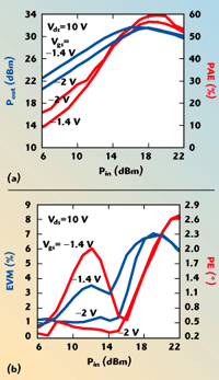
Fig. 9 Performance of the optimized PA2 at 2.21 GHz (a) Pout and PAE and (b) EVM and PE.
Conclusion
To achieve an output power of 25 dBm, the design started with WJAH102 and HMC454ST89 devices operating at a P1dB of 25 and 27 dBm, respectively. The EVM measured was less than 5 percent at 25 dBm. If the amplifiers are operated at 4 dB below or more from the P1dB, the EVM is improved to less than 2 percent. A new amplifier, based on an FLL177ME device, with P1dB of 32.5 dBm, was developed. Operating the FLL177ME with a 5 dB back off from P1dB, the PAE is almost the same as with the HMC454ST89 but the EVM improved to less than 1.5 percent. Based on the practical result measured, a linear PA can be achieved easily without linearization. The nonlinear distortion due to a PA can be minimized by selecting a PA device with a higher P1dB and operating at a lower DC current after it is matched for power using a load pull technique. The advantage of such an approach is that the designer can limit the drain current during load pull and match the PA device to the load impedance which gives the highest linear output power. For PAs with output power greater than 5 W, the proposed approach can be applied, but it is recommended to attach the PCBs directly onto the metallic housing using thermally and electrically conductive epoxy. It has been found that the grounding for very high power PAs might lead to lower power gain and output P1dB. In the worst case, the PA becomes potentially unstable and starts to oscillate.
References
1. A. Wright and W. Durtler, “Experimental Performance of an Adaptive Digital Linearized Power Amplifier,” IEEE Transactions on Vehicular Technology, Vol. 41, November 1992, pp. 395–400.
2. K. Konstantinou and D.K. Paul, “Analysis and Design of Broadband, High Efficiency Feed-forward Amplifiers,” IEEE MTT-S International Microwave Symposium Digest, 1996, pp. 867–870.
3. K.J. Parsons and P.B. Kenington, “The Efficiency of a Feed-forward Amplifier with Delay Loss,” IEEE Transactions on Vehicular Technology, Vol. 43, May 1994, pp. 407–412.
4. J.K. Cavers, “Adaptation Behavior of a Feed-forward Amplifier Linearizer,” IEEE Transactions on Vehicular Technology, Vol. 44, February 1995, pp. 31–40.
5. Y.W. Yeap, L.H. Chua and S.H. Tan, “Design of 3.5 W S-band Power Amplifier Based on Small Signal S-parameters Analysis,” Microwave Journal, Vol. 47, No. 7, July 2004, pp. 80–90.
6. “Ten Steps to a Perfect Digital Demodulation Measurement,” Agilent Product Note, PN 89400-14A, http://www.measurement. tm.agilent.com.
7. Y.Y. Wei, P. Gale and E. Korolkiewicz, “Effects of Grounding and Bias Circuit on the Performance of High Frequency Linear Amplifiers,” Microwave Journal, Vol. 46, No. 2, February 2003, pp. 98–106.
Yeap Yean Wei received his B.Eng. degree in communication and electronics engineering with first class honours from Northumbria University, UK, in 2002. Since December 2002, he has been working as a project officer at the Satellite Engineering Center of Nanyang Technological University. His main responsibilities include the development and integration of an X-band high bit-rate transmitter and a S-band telemetry and telecommand transceiver. His areas of research include power amplifier design, optimization of digital modulation circuit, and ultra wideband (UWB) signal generation and shaping. He can be contacted via e-mail at ywyeap@gmail.com.
Teh Eng Chuan received his B.Eng. degree in electrical and electronics engineering from Nanyang Technological University (NTU), Singapore, in 2004. He has been working as a project officer at the Satellite Engineering Center of NTU since August 2004. His current job responsibilities include the development and integration of a S-band telemetry and telecommand transceiver.
Chua Tai Wei received his BE degree in electrical engineering and his M.Eng. degree in engineering from Nanyang Technological University (NTU), Singapore, in 1992 and 1999, respectively. He is currently an assistant professor at the School of Electrical and Electrical Engineering of NTU. His current academic research interests include microwave circuit, signal processing in FPGA, and satellite engineering research and development. He is currently leading the Telemetry and Telecommand Sub-system in the NTU Satellite Engineering Center.