
High power broadband amplifiers are a crucial element for a variety of defense electronics and telecommunication systems. However, the product of power and bandwidth is fixed for a specific amplifying device, that is, the broader the bandwidth, the less the output power. Hence, a variety of broadband power combining techniques has been developed for achieving higher output power than is available from a single device.
Distributed amplifier designs have been widely used to achieve chip level solid-state amplifiers with a decade and greater bandwidth. This method sums the output power of a series of small devices while maintaining broad bandwidth by utilizing an “artificial” transmission line.1 However, a crucial limitation of this design for high power is that the device at the last stage must sustain the summed output signal; therefore, the total output power of a distributed amplifier is determined by the breakdown voltage of an individual device. Readily available GaAs pseudomorphic high electron mobility transistor (pHEMT) MMICs, covering 2 to 20 GHz, have breakdown voltages typically less than 20 V, resulting in about 0.5 W output power. Newly announced devices have breakdown voltages around 25 V, which sets a limit on saturated output power on the order of 1 W. The development of efficient combining methods is necessary to further increase the power capability of broadband amplifying systems and several approaches have been developed over the years.
In general, an N-way combiner can be represented as N parallel identical channels, as shown in Figure 1. Each branch of the combiner/divider is assumed to be identical and each output port gets the same amount of power. If the input port has a characteristic impedance of Zin, each separated parallel channel will have an input impedance of Zin•N. The output impedance for P1 to PN will remain as ZL. The key requirement of a good combiner is to design a broadband impedance transformer to match the impedance from Zin •N to ZL.

Fig. 1 An N-way divider/combiner representation (a) and its individual branches (b)
A typical transmission line impedance matching network is shown in Figure 2 with ZS being the input impedance and ZL the load impedance. Each section of the transmission line is a quarter wavelength at the center frequency. For a matching network with only one section of transmission line, the characteristic impedance of Zc is (ZS•ZL)1/2. The impedance ratio, Qr, which is defined as ZS/ZL, will determine the combiner’s bandwidth. Figure 3 shows simulation results for different Qr ratios.
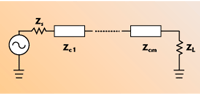
Fig. 2 Typical transmisison line matching network.
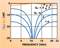
Fig. 3 Comparison of the bandwidth of a quarter-wave transformer for different impedance ratios.
To broaden the bandwidth, a multi-section quarter-wavelength transformer must be used to reduce the impedance ratio at each section. A Chebyshev equal-ripple passband transformer can be synthesized by manipulating the characteristic impedance of each section. The Chebyshev transformer is optimized to have minimum ripple inside the passband. However, to realize a 10:1 ratio transformer from 2 to 20 GHz, a 10-section transformer is required to achieve a –20 dB reflection coefficient, as shown in Figure 4.

Fig. 4 S-parameters of a 10-section 10:1 ratio Chebyshev transformer.
Typically, Zin and ZL are all 50 ?. As a result, Zin • N will be too high to be practically realized by planar circuitry when N is higher than 4. For N>4, a multi-stage combiner must be used. The problem here is that the resulting transmission lines will be extremely long in order to meet the bandwidth requirement, resulting in high combining loss and a physically large circuit. A fundamental limitation is that when a large number of devices are combined, a point of diminishing returns is reached where the combining losses approach the increased power anticipated by adding more devices.
Coaxial Waveguide Spatial N-way Combiner Design
The coaxial waveguide spatial power combiner addresses these bandwidth and loss issues by efficiently combining a large number of elements over a very broad bandwidth. Figure 5 shows the concept of a coaxial waveguide spatial N-way power combiner.

Fig. 5 Coaxial waveguide spatial N-way power combiner.
Here, a “tray” approach is used to build an amplifier using a coaxial waveguide N-way combiner. The amplifier system has a number of wedge shaped trays, each of which is 1/Nth of a cylinder. By radially mounting the wedge shaped trays, a coaxial waveguide structure is formed. Input and output coaxial waveguide tapers are used to feed the input of the coaxial waveguide structure and also to collect the output wave from the coaxial waveguide structure to an output port. Each wedge tray has circuit elements, which include an input broadband finline transformer, an active device, which is typically a MMIC amplifier, and an output broadband finline transformer. When trays are stacked together, the finline transformers are transformed into an array located between the inner and outer conductor of the coaxial waveguide structure. The transformer provides a match from the high impedance at the waveguide end to the active devices, typically 50 ?.
The N-way spatial combiner can still be described by the original representation. Instead of using planar circuits as in traditional combiners, however, the coaxial waveguide spatial combiner uses coaxial waveguide finlines for impedance matching. Since a coaxial waveguide is used, a TEM wave is propagating inside the waveguide. The coaxial waveguide finline is also a TEM transmission line, which has its own characteristic impedance. Conventional circuit theory can be used for matching and impedance transformation. Furthermore, because the characteristic impedance of a coaxial waveguide finline is very high, it is much easier to match from its high input impedance to the input of each active device.
There is very small dispersion even over a multi-octave bandwidth since the dominant mode that propagates along the coaxial line is TEM. The dense finline array helps suppress higher modes in the coaxial waveguide. The bandwidth of the transformer can be fully exploited because the coaxial waveguide does not have a cut-off frequency, as in a rectangular waveguide. Moreover, the uniform illumination of all the antennas helps to keep the amplifier system’s linearity much the same as for each individual MMIC amplifier. Since the minimum spacing between the trays is determined by the individual amplifier module size, the coaxial waveguide combiner has the benefit that the number of trays can be increased to provide very high output power. A high thermal conductivity metal is used for the wedge trays and this, along with the high thermal dissipation capacity of the tray approach, makes large-scale power combining feasible by enabling efficient and reliable heat removal solutions.
When the amplified signals from different MMICs are combined, the power is added since all the signals are in phase. But the residual phase noise from each MMIC amplifier is not correlated with that of the other modules. As a result, the phase noise at the amplifier system output is the same as for a single module, while the output power is N-times the power of a single module (less the combining loss), which can provide a substantial improvement in the ratio of carrier power to phase noise.
Amplifier System Power Supply
The power amplifier system uses an innovative biasing scheme, shown in Figure 6, to maximize the combining efficiency for the N-way spatial power combiner. Loss can be caused by amplitude and phase variations among the elements and the maximum combining efficiency will be achieved when all the MMICs have uniform performance. For the most part, the power modules use commercially available GaAs HEMTs, which can have significant variations from die to die at a fixed gate voltage. However, the gate voltage can be used to control the output current. To ensure each element is biased at the same current level, a feedback bias circuit is utilized to sense the drain current and lock it to a fixed value by adjusting the gate voltage. This serves to minimize output power variation across the large number of amplifying elements used in the array, which helps to improve the overall combining efficiency.

Fig. 6 Power supply for the coaxial power combining system.
High Power Amplifier Using Coaxial Waveguide Spatial Combiner Design
Figure 7 shows the complete amplifier system. It should be noted that the test unit was thermally designed so that it can be a platform for testing much higher power MMIC modules. The initial 10 W unit will fit in a standard 18 in. rack. Figure 8 indicates that the amplifier system exhibits flat small-signal gain across the 2 to 20 GHz band.

Fig. 7 A broadband, high power, coaxial waveguide combiner.
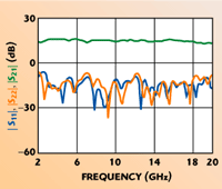
Fig. 8 Small-signal S-parameters.
Figure 9 shows the output power at the 1 dB compression point (P1dB) along with the saturated output power (Psat) over the frequency band (due to test equipment limitations, measurements above 18 GHz are not currently available). The sum of the Psat from each individual MMIC amplifier is also plotted as Psat_ideal, showing the system’s high combining efficiency.

Fig. 9 Psat and PldB as a function of frequency.
The exceptional combining efficiency has proved the commercial feasibility of several important design concepts for coaxial waveguide spatial combiners. First, very low loss can be achieved using coaxial waveguide finlines in a combining and dividing array. Second, the incident wave is evenly distributed to each channel and summed equally. Third, the regulation of the bias conditions of the individual amplifier elements ensures consistent output power across the entire array. All of these advantages result in an exceptionally efficient and reliable broadband amplifying system. In addition to high output power, the low noise figure (see Figure 10) and low intermodulation distortion (see Figure 11) result in a wide dynamic range for the amplifier system.

Fig. 10 Noise figure.

Fig. 11 Output power and IP3 as a function ofinput power.
Hermeticity and Power Amplifier Modules
Subsystems in defense electronic systems typically require survivability under adverse environmental conditions, with most systems requiring semiconductor devices to be hermetically sealed. While moisture seals using various plastic and epoxy materials are inexpensive and acceptable for most commercial applications, such methods are generally considered inadequate for most military standard specifications.
The coaxial spatial combining design uses stacked trays to form the waveguide opening. Hermetically sealing the entire system is not only an impractical approach from a cost standpoint, it makes it virtually impossible to service and repair the amplifier system. To overcome these problems, rather than sealing the entire system, each individual MMIC amplifier is hermetically sealed before its assembly into the system.
Broadband low loss packages using low temperature co-fired ceramic (LTCC) have been developed. To eliminate lead parasitics, a surface mountable approach is used. As shown in Figure 12, the package has a Cu/W base, which has a good match with the thermal expansion coefficient of the GaAs substrate material. The ceramic package is on top of the Cu/W base with a solder ring frame used to hermetically seal the package with another ceramic lid.

Fig. 12 The amplifier module assembly.
The package is resonant free from DC to over 20 GHz while maintaining low loss across the band, with the added benefit that the surface-mount approach greatly simplifies the assembly process.
Individual hermetic amplifiers are manufactured and tested before assembly into the amplifier system along with the individual bias stabilization and monitoring circuits.
Using solid-state devices combined with good thermal management results in high mean time between failure (MTBF), especially when compared with a TWTA. In the event of module failure, the amplifier output power and gain will gracefully degrade — “soft fail” — with the modular design lending itself to straightforward repair by replacing just the module.
Conclusion
The coaxial waveguide spatial power combining technique has resulted in a solid-state amplifier system that provides broad bandwidth and high linear output power. At 5 to 10 W across the entire 2 to 20 GHz band, it is believed to provide the highest power yet demonstrated with a commercially available solid-state amplifier. Employing off-the-shelf MMICs, the amplifier system combines 16 power amplifier modules, each of which has an output power of 25 dBm at P1dB and 26 to 28 dBm saturated. Using newer MMICs with a minimum saturated output power of 29.5 dBm, it is expected the units will provide 10 W minimum across the band. Importantly, the design is scalable; as higher power MMICs become available simply replacing modules will result in concomitant power output. For example, a 6 to 18 GHz amplifier has been built and tested, providing over 40 W of output power.2 Using this improved spatial combining technique, a power amplifier covering that band that is being developed, will provide greater than 50 W.
Coaxial space combined high power amplifier systems will soon be replacing broadband TWT amplifiers below the 100 W level with solid-state reliability, soft-fail characteristics, maintainability and improved power-added efficiency. While the primary applications are for the defense community in EW, ECM, ECCM, jammers, towed decoys and tri-band military satellite communications applications, commercial applications in research institutes for laboratory test systems and commercial test equipment markets can also be considered.
References
1. Y. Ayasli, L.D. Reynolds, Jr., J.L. Vorhaus and L.K. Hanes, “2–20-GHz GaAs Traveling-wave Amplifier,” IEEE Transactions on Microwave Theory and Techniques, Vol. 32, No. 1, January 1984, p. 71.
2. P. Jia, L.Y. Chen, A. Alexanian and R.A. York, “Broadband High Power Amplifier Using Spatial Power-combining Technique,” IEEE Transactions on Microwave Theory and Techniques, Vol. 51, No. 12, December 2003, pp. 2469–2475.
Pengcheng Jia received his BS degree in electronics science and information systems from Nankai University, Tianjin, China, in 1995, his MS degree in electronics engineering from Tsinghua University, Beijing, China, in 1998, and his PhD degree in electrical and computer engineering from the University of California at Santa Barbara in 2002. His research at UCSB involved the development of a waveguide-based broadband high power spatial power combiner. Since 2003, he has been with CAP Wireless Inc., Newbury Park, CA, as a senior member of the technical staff.