
Power, efficiency, linearity: pick any three — such a choice just about summarizes the challenges presented to the power amplifier (PA) designer in 2005. As wireless systems pack more data into limited bandwidths, power amplifiers carry a bigger burden but are still required to be efficient. Simultaneously, in order to maintain high information throughput from an ever-increasing number of users, the specifications on adjacent channel interference keep getting more stringent, and more efficient modulation systems keep demanding more dynamic range and higher instantaneous signal bandwidth. Meeting these challenges has evolved into an interesting blend of old and new techniques in device technology, PA architecture, and an ever-increasing intrusion of high speed digital signal processing (DSP) into the very traditional analog preserve of RF power engineering.
New Technologies and an Old One
“Swords into ploughshares” was the phrase we heard a lot in the early ’90s. Technologies that had been developed for, and largely funded by, the military were widely perceived as having potential for high volume commercial applications. In the world of RF semiconductors, the main candidate for such ‘military to commercial conversion’ programs was gallium arsenide (GaAs) semiconductor technology. Throughout the ’80s and ’90s, GaAs technology, in both discrete, hybrid and integrated forms, had stolen the show in RF amplifier applications. It had also seen a first wave of high volume commercial use in the LNAs of satellite TV receivers. The future for GaAs as the lead technology in the new wireless communications era looked very bright.
'From the PA viewpoint, things did not quite go to plan for GaAs fabrication shareholders. Two new transistor technologies emerged to dominate both ends of the mobile phone PA markets: silicon laterally diffused metal oxide semiconductor (LDMOS) for high power base stations and GaAs heterojunction bipolar transistor (HBT) for handsets. Neither technology would have attracted backers in the early ‘90s to dominate the scene in the way they have done; their emergence is an interesting case study. At the high power end, cost matters most, and although LDMOS needed careful stretching to meet performance goals at 2 GHz, the lavishly over-performing GaAs FET technology appeared to be more expensive on a dollar-per-watt basis. In the battery-powered environment of the mobile phone handset, the need for a single, unipolar bias supply and an ability to shut down in continuous receiving modes gave the bipolar HBT an important logistical advantage over the GaAsFET. In due course, some unexpected linearity advantages also emerged for a bipolar device in high crest-factor modulation applications.1
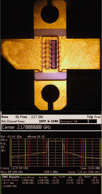
Fig. 1 100 W (CW)GaN device; ACP performance shown for 3GPP Test Model 1, 65 DPCH W-CDMA, 11 dB PAR; 15 W average power, 23.5% drain efficiency, 11.5 dB gain; package size is 20 mm × 6 mm. (Courtesy Cree Microwave Inc.)
The GaAs FET is not out of the picture, however. The availability of larger diameter GaAs wafers and more advanced fabrication machinery developed for sub-micron silicon processes have caused the emergence of the improved GaAs PHEMT, as a reliable high power option which shows significant efficiency and linearity benefits over LDMOS.
The emergence of LDMOS and the re-emergence of the GaAs pseudomorphic high electron mobility transistor (PHEMT), as preferred technologies for high power in the 2 GHz, 3G base station sector, have also had an impact on the opportunities for high bandgap semiconductors. Although long-touted silicon carbide (SiC) is finding some important niche applications, gallium nitride (GaN) seems to have taken over as the hottest and most promising of the new microwave power technologies.
Both seem to have more immediate advantages in broadband applications, although lessons learned from the HBT story would suggest that new technologies in the R&D laboratories can still make a rapid impact in commercial applications, if they have the right properties to do the job at hand. Figure 1, for example, shows a GaN FET device capable of 100 W, CW power, mounted in a 6 mm length package. This device has demonstrated 15 W average power in a 3GPP Test Model 1, meeting the adjacent channel power (ACP) levels shown at 23.5 percent drain efficiency for an 11 dB peak-to-average ratio (PAR).
An Old Problem, Three Old Solutions and a DSP-driven Revival
The problem of maintaining high efficiency and simultaneous linear operation is a very old one, dating back to the widespread growth of medium and short wave radio transmitters in the pre-World War II era. Consequently, there has been much recent attention paid to the revival of three classical solutions to this problem, which all carry the name of their accredited inventors: Kahn, Doherty and Chireix.2–4 It is probably a fair statement to say that just about any company or research group involved with PA design is putting major R&D efforts into at least one of these techniques at the present time.
An amplitude-modulated carrier only reaches peak envelope power (PEP) occasionally, and spends most of the time at an average carrier power level which is several times lower than the PEP level, an important property of the modulation scheme called peak-to-average ratio (PAR). This poses efficiency problems for a traditional class AB radio frequency power amplifier (RFPA), as shown in Figure 2. If the peaks are kept just below the clipping level, the average efficiency will correspond approximately to the efficiency of the PA at the mean power level, which can be several dBs lower than the PEP.
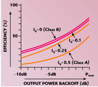
Fig. 2 Efficiency/power backoff performance of conventional class A, AB, B PAs.
So, although a 3 dB PAR may still suggest the possibility of achieving a mean efficiency in the 40 percent range, increasing the PAR to 6 dB sees this estimate drop into the 20 percent region. These rough estimates have to be taken along with the differing requirements for linearity in various applications. A GSM EDGE signal, for example, has a fairly low PAR (3 dB), but has an envelope profile that spends a much higher proportion of time at the peak levels, in contrast to conventional QPSK systems. This means that the PEP level has to be further backed off from the PA clipping level, and, from the efficiency viewpoint, a conventional class AB PA starts to look like a no-hope solution.
This problem is quite similar, whether we are dealing with a traditional AM transmitter or a modern multicarrier CDMA. Hence, the current research focus on reviving the three traditional solutions demonstrated by Kahn, Doherty and Chireix. The first of these, also known as ‘Envelope Elimination and Restoration,’ or EER, has become something of a generic term which is typically, and often inappropriately, applied to a variety of techniques that use supply modulation of a constant-envelope RFPA.
Figure 3 shows an envelope-construction PA system, which can be considered a modern derivative of the original Kahn transmitter. This architecture assumes that the baseband modulation is available and can be represented as orthogonal amplitude and phase modulation functions. A highly efficient PA is driven with a constant amplitude phase-modulated signal, and the amplitude modulation is achieved using modulation of the supply to the PA. This requires an additional high power component, which is a baseband PA, or power converter, whose efficiency must be included in the overall efficiency computation. Much of the recent research into the implementation of such a system has focused on this component.
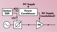
Fig. 3 Modern derivative of Kahn (EER) PA system.
The challenge in designing a suitable power converter escalates as the instantaneous bandwidth of the signal increases. This has been an inevitable trend in wireless communications. The OFDM signal in an 802.11a WLAN, for example, has a bandwidth of approximately 20 MHz. Progress is being made, however, in the innovative design of suitable baseband power converters.5
This focus on the power converter turns out to be something of a distraction from some other significant problems with this kind of system. In particular, the fundamental assumption that the saturated RFPA will pass the phase-modulated signal without distortion is seriously flawed. The supply modulation of the RFPA will inevitably impose some AM-PM on the original PM of the constant envelope input signal. The dynamic range of the amplitude control will also be an issue in zero-crossing modulation applications. Both of these problems can be attacked with DSP. The unwanted AM-PM can be reduced by suitable predistortion of the phase-modulated input signal, and the AM characteristic of the PA supply can be linearized using a digital look-up table (LUT). There is also the more generic problem that the system described is a complete transmitter, rather than a stand-alone PA.
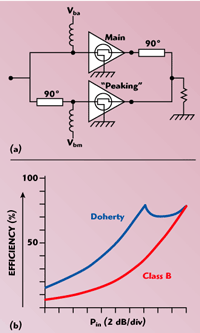
Fig. 4 Doherty PA (a) effiency performance compared to a conventional class B PA (b).
Figure 4 shows the Doherty PA (DPA), which, in its classical form, passes the test as a stand-alone ‘RF-in-RF-out’ PA. The basic action of a DPA is well covered in the literature.6 The technique has two key elements: the use of an auxiliary, or peaking, device, which only becomes active in the peak power regions of the modulation envelope, and the simultaneous modulation of the load seen by the main PA device in the peak power region. Over the last few years, there have been many papers that confirm that the classical efficiency characteristic of the DPA can be quite easily reproduced.
What is less clearly reported is the corresponding reduction in linearity that a practical DPA usually exhibits. In particular, some ‘crossover distortion’ in the region where the auxiliary device becomes activated can pose serious challenges even for a DSP predistorter. The peaking region will fundamentally show higher distortion levels, as compared to a conventional PA constructed using the same devices connected in parallel. This is because the load modulation of the main PA device maintains its output voltage swing close to the clipping level, whereas a conventional class AB PA would back away from clipping levels in this regime. Recent work7 has shown that some careful modifications in the basic design of the DPA can reduce these undesirable effects, to the point where a DSP predistorter can allow some of the most challenging CDMA multicarrier specifications to be met.
Of the various device technologies used for RFPAs, it is the GaAs PHEMT that has shown itself to be particularly well suited to exploiting the efficiency benefits of the Doherty configuration.7 The GaAs PHEMT can be biased off to make its output look very close to a totally reflective termination, something which an LDMOS device does less well. Figure 5 shows a Doherty PA module using GaAs PHEMTs, which is capable of 300 W PEP, 30 dB gain and a mean efficiency of 32 percent under multicarrier CDMA operation.
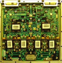
Fig. 5 GaAs PHEMT 300 W Doherty PA module. (Courtesy Filtronic, UK)
The Chireix outphasing system is shown in Figure 6. The basic action is easy enough to understand. The output of two efficient constant envelope RFPAs is power-combined so that amplitude modulation of the combined output can be affected by the introduction of differential phase modulation on the two input signals. In this simple view, however, there will be a large waste of power over most of the envelope amplitude range. In a classic 1935 paper,4 Chireix showed that there was a way around the efficiency problem.
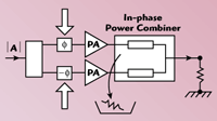
Fig. 6 Chireix outphasing PA system.
The use of a common load, rather than an isolated power combiner, allows for load modulation in an analogous manner to that used in the Doherty PA, using phase rather than amplitude modulation to achieve it. This load modulation causes a reduction in the current drawn by each PA device at lower envelope levels, and theoretically gives a power-backoff efficiency characteristic, which is similar to that of the Doherty PA. As indicated in the figure, this circuit modification can be achieved essentially by disposing of the isolation resistor in the combiner.
Although used at lower frequencies in high power broadcast transmitters, the Chireix technique has been treated with some suspicion by modern PA designers. Like the Kahn derivatives, it is fundamentally a transmitter technique, which requires full knowledge of the baseband modulation characteristics of the signal, and additionally some substantial signal processing to generate the required phase-modulated input signals. Such DSP horsepower has not traditionally been available in the cellphone handset environment. Wi-Fi (802.11) applications, however, pose an interesting and different perspective. The generation and processing of high speed data, that such applications require, opens up possibilities for implementing the more challenging requirements of an outphasing PA solution. Figure 7 shows a recently reported8 implementation of a Chireix outphasing PA for the 5 GHz, 802.11a band.
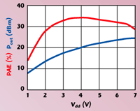
Fig. 7 Chireix outphasing PA for 802.11a applications. 6 (Courtesy IceFyre Semiconductor Corp., Canada)
Linearization: Old Memories, New Headaches
The development of linearization techniques for RFPAs has been an area of extensive research for many years, but more intensively so than ever in the last decade. As with PA design itself, we see older techniques re-emerging as useful solutions with the help of DSP. The last few years have seen an interesting contest between the traditional feedforward approach and a new player, digital predistortion (DPD). The contest has been particularly lively due to rapid improvements in high speed digital conversion and DSP hardware. This is starting to bring advanced DPD techniques into the handset/mobile PA zone, having previously been limited to high power multicarrier applications due to the high cost and power supply requirements of the high speed DSP and data conversion components.
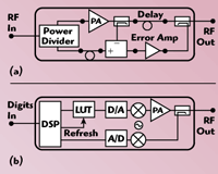
Fig. 8 PA linearization systems; feedforward (a) and digital predistortion (b).
Figure 8 shows both systems in basic form. The feedforward system generates a correction signal which is applied to the output; the correction signal is derived, on-the-fly, by subtracting a sample of the PA output from an undistorted input sample and amplifying the result in an error amplifier. A feedforward system in principle requires no knowledge of the signal, and can accept a modulated RF carrier as its only input. A DPD system applies a systematic predistortion algorithm to the PA input signal, which compensates for the ‘known’ PA distortion characteristics. Much effort over the last few years has shown that DPD is not very effective if based on a simple a priori look-up table (LUT). The predistortion algorithm needs to contain parameters that are continuously updated, or ‘refreshed’ to follow changes in the signal environment.
Most RFPAs display ‘memory effects,’ which means that their precise gain at any instant in time is not just a function of the input signal amplitude at the same instant, but somewhat dependent on the recent history of the input signal as well. This has been a major headache for DPD implementation, and has resulted in much greater complexity in hardware and software than was ever at one time imagined. A new term, predistortability, has emerged in the last year or so, as DPD implementers find, to their considerable frustration, that different PA designs have widely ranging amenability to digital correction.
Although much progress has been made in the understanding and correction of PA memory effects, the fast dynamics of wireless communications markets still springs surprises. One such unanticipated development was the deployment of High Speed Downlink Packet Access (HSDPA) in the 3G zones. The pulsed operation of this signal configuration caused problems for digitally predistorted PAs, whose adaption algorithms have trouble keeping up with the changes in PA properties caused by a pulsed signal environment. Thus, for 3G applications, it will be an important test of predistortability that specified linearity can be maintained over a range of signal dynamics without refreshment of the DPD coefficients. GaAs PHEMT designs have shown themselves to be very manageable under these conditions, as indicated in Figure 9.
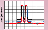
Fig. 9 A 400 W peak GaAs PHEMT Doherty PA's continous two-carrier W-CDMA signal (red) and the same signal at 10% duty cycle (blue) using the same DPD correction coefficients; average efficiency is 33% for 50 W mean power output. (Courtesy Filtronic, UK)
Broadband Pas: TWTs to GaN?
It comes as a surprise to many that tubes are still alive, if not especially well, in military electronic countermeasure (ECM) systems. The broadband requirements, such as coverage of a 1 to 20 GHz band in just two or three sub-bands, have limited the use of solid-state PAs to driver levels of a few watts. Traveling wave tubes (TWT), however, have been available for a decade or two, which can cover these wide bands at the 100 W output level, and at quite respectable efficiencies, in the 20 percent range. These applications would appear to be an obvious target for high bandgap semiconductors such as SiC and GaN.
However, the protagonists must beware of the turning of the tables; ploughshares can be turned back into swords. The recent re-emergence of GaAs PHEMT technology, coupled with the reliability track record GaAs technology, has established for at least two decades of military deployment, may yet freeze out the use of the newer emerging technologies, certainly in near-term rounds of TWT retrofit programs. But in the longer term, the potential of GaN technology is appealing in these applications.
Future Developments: The Digits are Closing In
It is a common experience for RFPA designers, most of whom have not been actively involved in the design or use of digital electronics, to be shown a PA concept such as that in Figure 10. This, we are told, is the ‘best’ way of generating a high power analog signal. Coding the input signal as a binary pulse-width modulated signal allows the use of a power switch rather than an amplifier, giving (it is further asserted) much higher efficiency than an analog RF amplifier. With the availability of digital hardware that clocks in the tens of gigahertz range, such well-established techniques should now be intensively researched for the direct generation of high power RF signals, so we are told.
Well, one might ask, are the digital folks right? The tentative answer is, yes, they may be right but possibly not for all the right reasons. There are some issues, which need to be clarified before pronouncements can be made that this is truly the way of the future for RFPAs operating at gigahertz frequencies. In particular there is the fundamental issue that regulatory conditions in the radio spectrum will not permit the direct transmission of high speed digital signals. For the foreseeable future, radio signals will be modulated carriers and the digital revolution will be restricted to the modulation component.
Fig. 10 Generations of a high power RF signal using digital drive to an RF power transformer.
Even the much-touted UWB standards are under pressure to revert to a band-limited format that removes some of the original ‘carrier-less’ concepts behind it. The world of RF airwave regulations is an analog one, and is likely to remain so for a long time, primarily due to major concerns about interference with existing services. So the high power digital output has to be converted back into an analog signal, which adds a number of complications to the original concept.
There are some interesting possibilities, however, and this may be an opening for high bandgap semiconductors, which can offer much higher power per unit device periphery (W/mm). Such devices, for a given power level, present correspondingly lower parasitic capacitances to the input and output circuits and the possibilities for driving them directly from fast logic would appear to be possibly an order of magnitude better than for existing GaAs or Si technologies. Once this interface has been achieved, things get more interesting. Improved methods for the digital encoding of a communications signal have been demonstrated that are less demanding on digital clock rates than simple pulse-width modulation, although it should be noted that this is a heavily patented area.
Conclusion
The next generation of PAs for wireless communications will utilize more advanced architectures and make extensive use of DSP correction. Conventional ‘stand-alone’ class AB PAs will become a rarer item, and will be limited to more specialized applications requiring broad RF bandwidths. The Doherty, Chireix and Polar/Kahn architectures will be necessary to boost the efficiency in high PAR and multicarrier modulation environments. PA designers may even be able to re-focus their efforts on the more exotic high efficiency modes due to the elimination of the linearity requirement in envelope-construction schemes.
The ‘new wave’ high bandgap technologies will have to work hard and get innovative to play a part in wireless communications PAs, but their future in TWT replacements for the military seems healthy. Meanwhile, the ongoing potential of more conventional silicon technology should not be underestimated. Sub-100 nm CMOS is now showing RF performance comparable to the GaAs MESFET devices available a decade ago, and CMOS RFPA performance appears now to be process, rather than device limited.
AcknowleDgments
The author wishes to thank R. Pengelly (Cree), R. Ranson (Filtronic) and G. Rabjohn (IceFyre) for supplying material for this article.
References
1. S.C. Cripps, Advanced Techniques in RF Power Amplifier Design, Artech House Inc., Norwood, MA, 2002, Chapter 1.
2. L.R. Kahn, “Single Sideband Transmission by Envelope Elimination and Restoration,” Proceedings of the IRE, Vol. 40, July 1952, pp. 803–806.
3. W.H. Doherty, “A New High Efficiency Power Amplifier for Modulated Waves,” Proceedings of the IRE, Vol. 24, No. 9, September 1936, pp. 1163–1182.
4. H. Chireix, “High Power Outphasing Modulation,” Proceedings of the IRE, Vol. 23, No. 11, November 1935, pp. 1370–1392.
5. F.H. Raab, “A Split-band Modulator for Kahn-technique Transmitters,” 2004 IEEE International Microwave Symposium Digest, pp. 887–890.
6. S.C. Cripps, RF Power Amplifiers for Wireless Communications, Artech House Inc., Norwood, MA, 1999.
7. I. Takenaka, et al., “A 240 W Doherty GaAs Power FET Amplifier with High Efficiency and Low Distortion for W-CDMA Base Stations,” 2004 IEEE International Microwave Symposium Digest, pp. 525–529.
8. J. Grundlingh, K. Parker and G. Rabjohn, “A High Efficiency Chireix Outphasing Power Amplifier for 5 GHz WLAN Applications,” 2004 IEEE International Microwave Symposium Digest, pp. 1535–1538.