
 High speed MMICs were historically developed for the United States military and included systems for high data rate network-centric communications, anti-jamming and low detection/interception warfare communications. The millimeter-wave frequency range provides benefits such as broader bandwidth, smaller antennas and greater security. Recently, military millimeter-wave activity has been overshadowed by the growth of commercial sector applications, such as point-to-point and point-to-multipoint radios, VSAT terminals, automotive radar, high speed digital communication networks, sensors and direct broadcast satellite television applications. With this shift, however, still comes a need for high volume Ka-band transmitters to address emerging and traditional military applications.
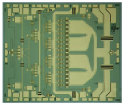
Mimix Broadband has developed two power amplifiers based on a new four-stage 34 to 37 GHz MMIC design. These power amplifiers utilize the company’s GaAs PHEMT device technology and electron beam lithography to ensure the highest level of repeatability and uniformity needed for both commercial and military applications. Robust thermal performance and standard 4 mil die thickness also make the device useful in both manual and automated assembly operations. The XP1072-BD multi-stage amplifier, Figure 1a, delivers over 35 dBm of pulsed saturated output power and 22 dB small-signal gain (see Figure 2a). The XP1073-BD device, Figure 1b, is a balanced amplifier version that provides over 37 dBm of pulsed saturated output power and 22 dB small-signal gain (see Figure 2b).

Figure 1 Photo of XP1072-BD (a) and XP1073-BD (b).

Figure 2 XP1072-BD (a) and XP1073-BD (b) measured on-wafer gain.
Performance
The XP1072-BD operates on a recommended drain voltage of 5.5 V DC and a nominal -0.7 V DC on the gates. Separate biasing of the stages within the amplifier is recommended if the amplifier is to be used in a linear application or at high levels of saturation, where gate rectification will alter the effective gate control voltage. For non-critical applications it is possible to parallel all stages and adjust the common gate voltage for a total drain current Id (total) = 2400 mA (maximum 3.0 amps). The power added efficiency for the single die version is 25 percent and 24 percent for the balanced version. The rated operating temperature of the device is between -55° and +85°C.
For applications such as radar, where the amplifier RF output power is saturated, the optimum drain current will vary with RF drive and each amplifier stage is best operated at a constant gate voltage. Significant gate currents will flow at saturation and bias circuitry must allow for drain current growth under this condition to achieve the best RF output power and power added efficiency. Additionally, if the input RF power level varies significantly, a more negative gate voltage will result in less die heating at lower RF input drive levels where the absence of RF cooling becomes significant. Note under this bias condition, gain will then vary with RF drive. Output power as a function of frequency is shown for both devices in Figure 3, demonstrating the amplifier’s performance.

Figure 3 XP1072-BD (a) and XP1073-BD (b) output power.
For linear applications where optimum IM3 (Third-Order Intermod) performance is required at more than 5 dB below P1dB, active gate biasing can be implemented to keep the drain currents constant as the RF power and temperature vary. Active biasing of the gates gives the best performance and most reproducible results. Depending on the supply voltage available and the power dissipation constraints, the bias circuit may be a single transistor or a low power operational amplifier, with a low value resistor in series with the drain supply used to sense the current. The gate voltage of the PHEMT is controlled to maintain the desired drain current and provides an indirect form of temperature compensation.
Applications
These amplifiers focus on serving market applications where performance (saturated power and PAE), compact size and extreme ruggedness are primary drivers. While new applications are emerging, RADAR is probably the most closely targeted application, using FMCW on missiles and munitions. Another likely defense application is Ka-band for battlefield resource tracking and management. Airborne applications include landing systems for commercial fixed wing aircraft and precision altimeters for rotary craft on the military side. In many cases, these parts will reside behind small antenna elements or arrays on small platforms and therefore the devices are offered in die form as preferred by most of the system integrators working at these frequencies and power levels.
While lower power MMIC solutions are currently available, these devices are limited to power levels that in the past required 2 or 4 way combining to achieve the required output power. Due to circuit losses, combining lower power devices leads to diminished performance, hurting overall power and efficiency while increasing the substrate footprint. Conversely, combining with this device raises the ceiling of what was thought possible with solid-state amplifiers. Multiple die combined in an array provide a solid-state solution for RADAR applications. Multiple gain stages eliminate drivers, and the balanced design offers better VSWR and greater power from a single part. Power combining naturally becomes more painful as you go up in frequency. This device eliminates or reduces the need to combine die in many applications. With a reduced part count, using these MMICs to design high power solid-state amplifiers offers the benefits of lower complexity and simpler assembly, leading to higher yield and optimal results.
Mimix Broadband Inc.,
Houston, TX (281) 988-4600,
www.mimixbroadband.com.
RS No. 301