
Advancements in Vector Network Analysis (VNA) hardware and software algorithms have enabled a new class of instrumentation for analysis of active components. The Nonlinear Vector Network Analyzer (NVNA) performs a variety of measurements for a number of different application areas. These measurement applications are of importance for those designing active components such as amplifiers and in general any component that exhibits nonlinear behavior. The NVNA can also be used to analyze complex signal behavior while applying VNA error correction providing extremely accurate signal analysis capabilities. The NVNA provides vector corrected measurements of the absolute amplitude and cross-frequency phase of frequencies to/from the component with the highest level of accuracy.
Mathematical Representation of Frequency Spectrum
Generally a VNA measures and displays data in the frequency domain. One example is scattering coefficients (S-parameters) of a component versus frequency. The S-parameters are coefficients of a linear model and are ratios of absolute quantities where the stimulus frequency is the same as the response frequency. Figure 1 illustrates a simplified two-port VNA. The VNA measures the ‘a’ and ‘b’ waves at both ports of the component at the same frequency, applies error correction to move the reference plane to the component level, and then typically takes ratios of these waves to generate the S-parameters. However, if a component exhibits nonlinear behavior, there may not be a one-to-one relationship between the input and output frequencies (see Figure 2). In addition, the definition of S-parameters becomes invalid and cannot be used to accurately describe the component behavior. In this case, it is important to accurately measure the vector corrected absolute amplitude of the frequencies and the phase relationship between frequencies (cross-frequency phase) of the ‘a’ and ‘b’ waves. Traditional VNAs do not have the ability to accurately measure these characteristics. The NVNA, however, can make these measurements with the highest level of accuracy. Once these absolute quantities are measured, they can then be used to analyze component and complex signal behavior.

Figure 1 Schematic of a two-port VNA.

Figure 2 Nonlinear component behavior.
Nonlinear Vector Network Analyzer Architecture
The NVNA is based on the Agilent PNA-X series of VNA. It consists of an integrated NVNA firmware application that transforms the PNA-X VNA into the NVNA (see Figure 3a). A simple three-step calibration process using a new phase calibration standard (see Figure 3b), a vector calibration with a vector calibration kit, and amplitude calibration with power sensor, provide the ability to calibrate and measure the vector error corrected absolute amplitude and cross-frequency phase stimulus/response information of components or signals. The PNA-X can be switched to the standard VNA mode or the NVNA mode simply by running the integrated application of choice on the instrument.

Figure 3a Nonlinear vector network analyzer (NVNA).

Figure 3b New phase calibration standard.
The new phase calibration standard provides the means to acquire error corrected cross-frequency phase information from the component that is traceable to standards labs. It operates over the frequency range of the PNA-X and has the ability to generate a frequency grid spacing of less than 1 MHz. This grid spacing sets the minimum frequency step for the measurements. It is very insensitive to temperature, input power and drive frequency providing stable and accurate measurements and calibration.
A segment table in the NVNA provides the ability to generate a multi-dimensional stimulus/response sweep. As an example, a sweep plan can be configured where the RF stimulus is swept from 1 to 2 GHz over 11 points, the RF power swept from -20 to +10 dBm over 31 points, and the receivers configured to measure 5 harmonics at each of the stimulus settings. This means there are a total of 11 x 31 x 5 = 1705 measurement points. The NVNA also can control external instrumentation synchronously with the RF measurements to read parameters such as DC voltage and current.
Nonlinear Vector Network Analyzer Measurement Applications
The NVNA has a number of new measurement applications. All of these measurement applications have the highest degree of accuracy since vector error correction is applied thus removing the systematic measurement errors such as impedance mismatch and loss. The NVNA enables these applications due to the ability to relate the amplitude and phase (cross-frequency) between the stimulus/response frequencies that are measured with this error correction applied.
Absolute Amplitude and Cross-frequency Phase
The NVNA can measure the vector corrected absolute amplitude and cross-frequency phase stimulus/response information from the component. Figures 4a and 4b illustrate a measurement of an amplifier driven into compression with a 1 GHz stimulus at -6 dBm. The ‘a1’ wave is the incident wave applied to the component, which shows a very large response at the 1 GHz fundamental frequency and very low responses at the harmonics. This is because the source harmonics from the PNA-X source are well below -60 dBc. The ‘b2’ wave, which represents the output from the component, contains harmonic content due to the nonlinear behavior of the component. The vector corrected absolute amplitude can be measured as well as the phase relationships between all the frequencies. As an example, the cross-frequency phase between the fundamental and second harmonic on the ‘b2’ wave is shown to be 122.1°. Since the amplitude and cross-frequency phase of all the frequency spectra is accurately known, an inverse Fourier transform can be applied to the frequency domain data to generate the time domain waveforms, as shown in Figure 4c.

Figure 4a Component amplitude stimulus/response in frequency domain.

Figure 4b Component cross-frequency phase stimulus/response in frequency domain.

Figure 4c Component stimulus/response in time domain.
Vector Corrected Time Domain Scope
The NVNA can be used as a vector corrected time domain scope by measuring the absolute amplitude and cross-frequency phase of the signals with error correction applied. Measurements are made in the frequency domain and an inverse Fourier transform is applied to get the time domain waveforms. The NVNA with the N5242A PNA-X can sweep from 10 MHz to 26.5 GHz. The NVNA can then be used as a vector corrected time domain scope with 26 GHz of detection bandwidth. A general ‘rule-of-thumb’ is that the resolution in the time domain at each discrete point is inversely proportional to the swept bandwidth (1/(26 GHz) ≈40 ps). Figure 5 illustrates a measurement of an amplifier driven into compression. The yellow trace is the input sinusoidal voltage waveform at the component terminals and the blue trace is the compressed output voltage waveform. The output waveform is distorted due to the presence of high harmonic levels that are generated by the component.

Figure 5 Component stimulus/response voltages in time domain.
RF I/V Curves
Often, RF I/V curves are used to analyze linear and nonlinear characteristics of a component, such as an amplifier. These curves are often superimposed on the DC I/V curves (which set the component operating point) and provide the designer important information on the component behavior under various DC bias and RF conditions. An example would be measuring the time varying drain voltage (Vd) in conjunction with the time varying drain current (Id). At each instance in time, the drain voltage and current are compared and displayed as in Figure 6. These voltage and currents are calculated based on the measured ‘a’ and ‘b’ waves as in Equation 1.


Figure 6 Component RF I/V response.
Multi-tone Stimulus/Response
In some scenarios a multi-tone stimulus is likely to be applied to the component to subject it to a spectrally rich stimulus thus exciting more nonlinear behavior. Figure 7 illustrates a measurement of an amplifier with an input stimulus of 5 frequencies, spaced 10 MHz apart and centered at 1 GHz. The NVNA measured the entire resulting spectrum (multi-tone and inter-modulation products at the fundamental and harmonics) out to 26 GHz, and then performed an inverse Fourier transform to get the time domain response. Nonlinearity is clearly evident when comparing the ‘a1’ waveform envelope (input stimulus) to the ‘b2’ waveform envelope (output response) of the amplifier.

Figure 7 Component amplitude response in time domain with multi-tone stimulus.
Fast RF and DC Pulses
The NVNA can be used to analyze complex signals. To illustrate this application a very narrow DC and RF pulse is measured. To visually generate what the spectrum of a pulsed signal looks like, the time domain response is first mathematically analyzed. Equation 2 (time domain view of pulsed signal) illustrates the time domain relationship of a pulsed signal. This is generated by first creating a rectangular windowed version (rect(t)) of the signal with pulse width (PW). A comb function is then realized consisting of a periodic train of impulses spaced 1/PRF apart where PRF is the pulse repetition frequency. This can also be viewed as impulses at spacing equal to the pulse period. The windowed version of the signal is then convolved with the comb function to generate a periodic pulse train in time corresponding to the pulsed signal, as illustrated in Figure 8.

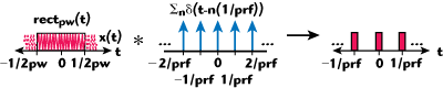
Figure 8 Time domain representation of a periodic pulsed DC signal.
Equation 3 (Fourier transform of time domain pulsed signal) illustrates that the frequency domain spectrum of the pulsed signal is a sampled sinc function with sample points (signal present) equal to the pulse repetition frequency (from the comb function).
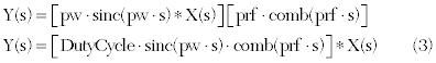
Figure 9 shows what the pulsed spectrum would look like for a signal that has a pulse repetition frequency of 2.5 GHz and a pulse width of 40 ps with no carrier modulation (pulsed DC). Notice that the spectrum has components that are n x PRF away from the modulated signal (DC or RF). If it is pulsed DC then the spectrum is centered on DC (X(s) = DC). If it is pulsed RF, the spectrum is centered on the pulsed RF carrier (X(s)). It also contains null points that are spaced n/PW. Extremely narrow pulse measurements are possible with the NVNA due to its 26 GHz of vector corrected detection bandwidth, which corresponds to a minimum resolution in the time domain of approximately 40 ps.

Figure 9 Frequency domain of periodic pulsed DC signal.
Figure 10 shows a measurement of a DC pulse with PW less than 50 ps. Figure 11 illustrates an RF pulse measurement where the pulse width is 10 ns and the carrier frequency 2 GHz. Figure 12 shows the measurement of a square wave.

Figure 10 Measurement response of a pulsed DC signal in time domain.
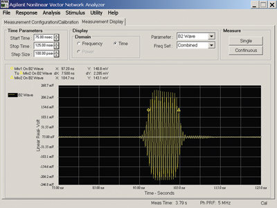
Figure 11 Measurement response of a pulsed RF signal in time domain.

Figure 12 Measurement response of a square wave signal in time domain.
Another possible measurement would be multipath responses in an antenna chamber when measuring the RCS of an object.
Multi-envelope Domain
A nonlinear component may exhibit dynamic memory effects. Memory effects in an amplifier can cause distortion that is undesirable. To measure and analyze memory effects, a multi-envelope measurement can be performed where the component is stimulated with a pulsed signal (RF and/or DC bias) and the resulting envelope ‘a’ and ‘b’ waveforms are measured at the fundamental and harmonics frequencies. The envelope amplitude and phase can be analyzed versus time at each of the spectral components. If the component exhibited no memory effects, then the envelopes from the component would not have a time varying phenomena (that is the envelope would be flat). Figure 13 shows an amplifier that exhibits both nonlinear behavior and memory. A 1 GHz pulsed RF stimulus was applied to the component with a pulse width of 100 us. Harmonics are generated by the component due to its intrinsic nonlinearities. Each fundamental and harmonic has a distinct envelope profile due to the dynamic memory effects in the amplifier. Short-term memory dynamics as seen at the beginning of the pulse may be caused by bias network memory and longer term slopes in the envelope may be caused by thermal memory. The NVNA can measure down to envelope resolutions of 16.7 ns in standard mode.

Figure 13 Component multi-envelope domain response.
X-parameters
A typical VNA can measure scattering coefficients of a component often called S-parameters. Equation 4 illustrates the S-parameter model and equations for a two-port component.

The S-parameters describe the linear behavior of the component and can then be used to design predictable linear systems. When measuring a component that exhibits nonlinear behavior the definition of the linear scattering model is no longer valid. In such a case, where the component has multiple input and output frequencies, due to linear and nonlinear behavior, a new model must be generated that encompasses both the linear and nonlinear characteristics of the component. Equation 5 shows this new model with scattering coefficients called X-parameters (LSOP = Large Signal Operating Point).

i = output port index
j = output frequency index
k = input port index
l = input frequency index
The X-parameters are the logical, mathematically correct extension of S-parameters into a nonlinear large-signal operating environment. The X-parameters fully describe the input and output frequency mapping of the component and/or system thus completely describing the linear and nonlinear behavior. The NVNA measures the X-parameters of the component that can be displayed as well as imported into Agilent ADS as a fully operational linear and nonlinear model for optimization, simulation and design.
The X-parameters can provide information such as the component gain and match, while the component is operating in a linear or nonlinear state. The X-parameters can then be displayed like S-parameters (see Figure 14). Since the X-parameters relate cross-frequency dependences, there can be many more X-parameters than S-parameters. As an example, the response of the output fundamental to the input third harmonic input is X21,13. In addition, X-parameters depend explicitly on the large-signal state of the component, so input power may be a variable, unlike S-parameters that are assumed to be power independent. Possibly one of the strongest benefits of X-parameters is the ability to accurately cascade the X-parameters from individual components using ADS to design and simulate more complex modules and systems.

Figure 14 Component X-parameter behavior.
The usefulness of the X-parameters can be illustrated in the process of designing a power amplifier. The designer is compelled to drive the amplifier into the nonlinear region to get the maximum output power as well as to extract the maximum efficiency. Some form of a feedback circuit is then used to compensate for the nonlinear effects and make the output behave like a high power linear component. A typical approach is to suppress the harmonic outputs of a power amplifier using filters and other components. If the input match of the filtering components is not appropriately matched to the output match of the specific harmonic of interest generated by the amplifier, then the attenuation level of that specific harmonic could be significantly different than anticipated. This leads to a time consuming iterative design experience where the maximum performance of the component may never be fully realized. With accurate phase and amplitude information from the X-parameters and using simulation tools, designers can design the most robust systems possible in the shortest amount of time, with the highest degree of accuracy.
Conclusion
The NVNA has enabled a number of new measurement applications. Component behavior and complex signal analysis can be analyzed in the time, frequency and power domains with vector error correction applied. Memory effects can be analyzed utilizing the multi-envelope domain and the new nonlinear scattering coefficients (X-parameters) can be measured and then used for design and analysis of active components and systems.
References
- Agilent Technologies, www.agilent.com/find/nvna.
- Agilent Technologies, “PNA/PNA-X Series Microwave Network Analyzers,” Agilent Technologies Configuration Guide 5988-7989EN.
- “Polyharmonic Distortion Modeling,” IEEE Microwave Theory and Techniques Microwave Magazine, June, 2006.
- “Vector Harmonic Amplitude/phase Corrected Multi-envelope Stimulus Response Measurements of Nonlinear Devices,” IEEE MTT-S 2008.
- “Measurement-based Large-signal Simulation of Active Components from Automated Nonlinear Vector Network Analyzer Data via X-parameters,” COMCAS 2008.
- Agilent Technologies, “Pulsed-RF S-Parameter Measurements Using Wideband and Narrowband Detection,” Agilent Technologies Application Note 5989-4839EN.
- Agilent Technologies, “Pulsed Measurements Using the Microwave PNA Series Network Analyzer,” Agilent Technologies White Paper 5988-9480EN.
Loren Betts received his BSc degree in computer engineering from the University of Alberta, Edmonton, Alberta, Canada, in 1997, and his MSc degree in electrical engineering from Stanford University, Stanford, CA, in 2003. Currently he is completing his PhD degree in electrical engineering from The University of Leeds, Leeds, UK. His PhD. research is specifically the invention and development of the Nonlinear Vector Network Analyzer (NVNA). He won the “Barnholt Innovation Award” for the NVNA as the invention of the year at Agilent Technologies in 2008. He is currently a research scientist at Agilent Technologies focusing on complex stimulus/response measurements and modeling of nonlinear components utilizing vector network analyzers. He invented and developed the pulse measurement detection algorithms utilized in current Agilent VNAs as well as the NVNA from Agilent. He was also instrumental in driving the current multiport measurement and control schemes used in current Agilent VNAs as well as antenna measurements.