

Until recently, traveling wave tube (TWT) technology was the only technology capable of meeting the bandwidth and power requirements of high power L-band applications such as power testing radar components and for military/automotive RF immunity testing. Solid-state technology can, however, offer key performance advantages over TWT technology, particularly with regard to harmonic levels, linearity, gain flatness, mismatch tolerance and improved maintainability/reliability. But the task of developing octave band microwave power amplifiers that are cost competitive has been an elusive goal. That goal has been achieved by MILMEGA with the development of the AS0102-800, a solid-state amplifier delivering over 1 kW in the 1 to 2 GHz band.
The AS0102-800 Architecture
The unit was developed using the company’s favored amplifier topology — the Corporate Structure Amplifier (CSA). It derives its name from the hierarchy of levels employed in its construction, which, ignoring the combining elements, gives the block diagram of the amplifier an appearance not dissimilar to that of a rotated company organizational chart (see Figure 1).
The usual form of a CSA employs identical unit amplifier designs within each level, or rank, of the hierarchy, but designs may vary from rank to rank. Typically, a lower power, high gain, unit amplifier (a pre-amplifier) is employed at the front end of the amplifier system with higher power, lower gain units being employed in the output rank. All the useful power in a CSA is developed in the output rank, the preceding ranks being used only to develop the required drive levels.

Fig. 1 Corporate Structure Amplifier schematic.
The AS0102-800, which is available in forced-air or water-cooled versions, follows the CSA philosophy. The final design consists of 32 power modules in parallel, arranged in banks of eight, with each of these banks having its own driver module, the four banks of eight being combined with a very low loss combiner. The key microwave components of the amplifier system are the output rank power modules and the final combiner that must be capable of handling in excess of 1 kW of CW power, across an octave bandwidth (1 to 2 GHz).
The Output Rank Power Module
The building block of the amplifier’s output rank is the company’s AS0102-35M, a GaAs FET-based 1 to 2 GHz 35 W power module, with a typical gain of 20 dB. Concentrating on the development of a single power module has the virtue that a high percentage of engineering resource, microwave, electrical, mechanical, thermal and reliability can be focused to design an outstanding component around which a system can then be built. Figure 2 shows the module construction.
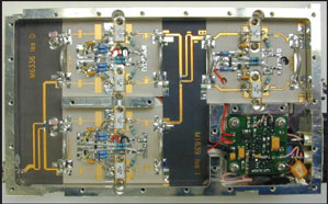
Fig. 2 35 W output rank power amplifier module construction.
Power is developed within the module by combining two 20 W balanced pair amplifiers. Using one level of broadband quadrature combiners, plus the use of a robust GaAs FET technology, allows the modules to absorb 100 percent reflected power even when the module is operating at full output power. This can be a significant benefit to the system designer if the amplifier system is required to operate into high VSWR conditions.
Developing the 250 W Block
With the development of the output rank power module complete, the next stage was to develop a quarter section. This required the parallel combining of eight power modules. A schematic representation is shown in Figure 3, along with the results achieved from combining eight modules by this method. Partitioning the final amplifier in this way greatly eases maintenance in the final system.

Fig. 3 The 250 W quarter section’s (a) schematic and (b) performance.
The Output Combiner
The development activity set out to improve on an existing MILMEGA design, which was implemented as a conventional stripline combiner using 2 × 0.25 inch thick Duroid slabs. The aim for the new combiner was to reduce losses and improve general manufacturability of the component. A 3D view of the board layout, showing routing slots, is illustrated in Figure 4. The losses incurred in the existing 1 kW combiner were around 0.4 dB, which equates to a loss of 100 W of valuable microwave power. This power loss also created a heat problem, which required the use of a large heat sink to ensure effective dissipation, setting a limit on the physical size of the resultant structure.

Fig. 4 3D view of the output combiner board layout.
In investigating an alternative design, the focus was on the causes of losses, which were recognized as substrate-dielectric losses, copper losses in the tracking and connector losses. After some investigation, it was decided that a suspended stripline solution would offer the best trade-off in terms of losses and mechanical dimensions. Air was the chosen dielectric.
Power combining of the four 250 W inputs is implemented using a two-layer cascade of two input resistorless Wilkinson style combiner structures. The resistors are not required in this application because all input signals are assumed to be matched in both phase and amplitude. The completed combiner/coupler operates over the 1 to 2 GHz range and has an integrated directional coupler, which provides forward and reverse outputs for sampling and measurement of incident/reflected power. Because of the high powers involved, each 250 W input connector is an N-type. The output connector is a 7/16-inch type. Figure 5 shows the measured transmission responses of the combiner. Note the flatness of the amplitude response and the low insertion loss. This new combiner design produced less than half the loss of the existing design and, in tests with a full 1 kW of RF power being produced, the heat dissipation in the component was negligible.

Fig. 5 Measured performance of the output, 1 kW combiner.
The Final System
The power achieved in the final system is shown in Figure 6, with a minimum of 1 kW of saturated power achieved across the band 800 MHz to 1.95 GHz, which is in excess of an octave bandwidth. For a major proportion of this band, this power is of the order of 1.3 kW. Also of note is the close tracking of the 1 dB compression level to the saturated power level, allowing the amplifier to deliver up to 6 dB more linear power than the TWT equivalent.

Fig. 6 Final stage of the 1 kW power amplifier; (a) schematic and (b) measured output power.
Inherent Reliability
The multi-module combining approach in the output rank ensures that there is a low probability that a single random failure will cause the amplifier to cease operating in a satisfactory manner. It is more likely that failure modes will cause a gradual and predictable reduction of power over a period of time until a level is reached at which its performance has degraded below an acceptable threshold. This attribute is called ‘graceful degradation’ and is an intrinsic benefit of amplifiers developed with a CSA philosophy. For the output rank of the amplifier, the loss in microwave power is related to the number of failures by the equation:
Power loss = 10 log [Ns/No]2 (dB)
where
Ns = the number of surviving modules
No = the number of original modules in the output rank
For the AS0102-800, which has 32 modules in the output rank, if one module fails the output of the amplifier drops by 0.28 dB. If one transistor fails the output power drops by only 0.07 dB, demonstrating the minimal effect that a single transistor failure has on an amplifier of this type. Both scenarios allow the user to continue using the amplifier until a suitable shutdown/maintenance period has been reached. This ability to defer maintenance to a time when cost is minimal is one of the major benefits of the amplifier when compared to a TWT equivalent.
Conclusion
The AS0102-800 is a unique, octave bandwidth, solid-state microwave power amplifier, competing successfully in technical and cost performance with TWTs for the delivery of 1 kW across the 1 to 2 GHz band. In addition, backed by the company’s five-year warranty, it represents a major step forward for solid-state power amplifiers.
MILMEGA Ltd.,
Isle of Wight, UK,
+44 1983 618004,
www.milmega.co.uk