
The future of wireless communications is about its evolution from a technology to a resource—as common to our experience as water and electricity. In order to get there, though, the industry has to overcome some significant design challenges in mobile devices, many of which will be helped by advancements in semiconductor technology. Today’s consumer mobile devices can include as many as nine RF chains, and engineers are taxed to meet the size, power and coexistence requirements of next-generation form factors.
While many of us tend to focus on the evolution of networking technology standards and technologies as the driver of ubiquitous wireless (EDGE or 1xRTT? LTE or WiMAX? Satellite-based or terrestrial-based? Single-carrier or multi-carrier?), the reality is that the future of wireless communications is as much about the consumer device as it is about the network on which the device operates. The future of wireless communications is about how seamlessly wireless capability—and, most critically, RF technology—integrates into the various devices, vehicles, tools and spaces defining our daily lives. In addition, next-generation designs must be able to keep up with changing usage models. For instance, few predicted the explosive growth of text messaging, and dramatic improvements in RF and SoC capability and power consumption have enabled a richer mobile Internet browsing experience. Many are now focused on adding location-based services to mobile handsets, and the mobile device needs to have the required RF circuitry to handle all of these diverse signal chains.
Innovation Required
Seamless inclusion of wireless communications into our day-to-day existence has, until recently, often frustrated the best efforts of the wider electronics industry. Often referred to as “the black art of electronics,” RF signal processing has long resisted the transition from circuit board-based discrete components to IC subsystems. Discussions of “the future of wireless communications” over the last decade have often referenced relatively exotic RF physical layer architectural innovations such as “software-defined radio” and “polar modulation,” implying that fundamental rethinking of the approach to RF signal processing represented the best path to wireless pervasiveness.
Instead, the future of commercial wireless communications lies not with exotic architectures, but with fundamental advances in how we use existing semiconductor manufacturing technologies. If the microprocessor industry has taught the RF industry anything, it is that, when done well, system-level functional integration enables lower power consumption, increased performance and smaller component footprints. As the user’s experience of a wireless service is defined by the performance of the device, so the performance of the device is defined by the quality of the RF physical layer. The future of wireless communications lies with innovations in RF physical layer integration on the scale achieved for the operational amplifier in the 1970s: reliable, repeatable performance; standardized interfaces; user-programmable functionality; and ease of manufacture. Borrowing from the software industry, the promise of truly ubiquitous wireless requires a “plug-and-play” RF physical layer.
Integration Opportunities
A crucial impact on the future of wireless communications comes from the transition to multi-carrier orthogonal frequency division multiplexing (OFDM) modulation as a means for gaining increased bandwidth from a scarce worldwide spectrum resource. All next generation radios will be based on OFDM, including those used in Long Term Evolution (LTE) mobile handsets, WiMAX and WLAN systems. OFDM most notably results in high peak to average power ratios, which drives a need for higher efficiency RF power amplifiers.
The interrelationships between signal processing quality, power consumption and transmit power/receiver sensitivity are complicated by the requirements of OFDM signal processing for the RF physical layer.1 Yet, along with these inherent challenges, the transition to OFDM provides the opportunity to develop converged multi-mode RF physical layer functionality. As high-bandwidth wireless content is delivered to a wide variety of consumer platforms, system designers will need the RF physical layer to have “operational amplifier-like” qualities, meaning it will need the ability to be optimized for specific requirements and self-compensate performance for wide variations in operating conditions.
An op amp integration model for RF would also invite collaboration between numerous product and technology partners, such as what has occurred at the content processing level. This will surely stimulate innovations that will improve the wireless experience. The rapid introduction of navigation as a mobile phone application was made possible by the relative ease of introduction of the GPS hardware solution onto the mobile phone platform. As GPS becomes integral to the mobile phone, applications and operating systems will better integrate navigation and other location-based services into the mobile phone experience.
For instance, if mobile handsets could support more bandwidth, Google maps could download fast enough to provide real-time information while driving, and still leave enough power to make a phone call (see Figure 1). RF physical layer integration on par with that of the op amp will enable the types of collaboration necessary to continue integrating wireless services into the full range of daily activities. But how do we get there?

RF Plug and Play
As a matter of fact, this concept of RF “plug-and-play” is already becoming a reality. For instance, location-based services in mobile phones have been eagerly anticipated for almost a decade. Although CDMA phones have incorporated GPS-based baseband signal processing since their inception, the need for high receiver sensitivity (roughly –160 dBm) and near-frequency high-power interference from cellular signals created a natural impediment to small footprint, low-power GPS solutions for full-featured, location-based consumer services. However, this all changed with the introduction of high performance, low power consumption, integrated RF physical layer GPS receivers that are capable of co-existence with cellular networks (see Figure 2). Their release has been the catalyst for rapid integration of GPS-based navigation services in mobile phone platforms.
The need for WLAN functionality in handheld devices led to the convergence of WLAN, FM radio, GPS and Bluetooth technologies onto single digital signal processing platforms. We are now seeing multi-function RF front ends—combining the power amplifier, low noise amplifier, RF switch and filtering in a single package, creating multi-mode RF signal processing solutions. These higher levels of integration and modularization are made possible by semiconductor technologies such as silicon germanium (SiGe), which enables single-chip mode-programmable RF front ends with the RF performance, low power consumption and small form factors required for thin, display-centric devices similar to Apple’s iPhone.® The end result of RF plug-and-play integration will be a rich suite of wireless connectivity-based applications—in-car navigation systems with roadmaps showing location through GPS, local traffic using FM radio data system (RDS), which is linked to the car’s audio system via Bluetooth, and the ability to upload audio and video entertainment via WLAN.
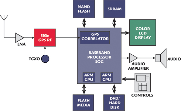
The migration of RF signal processing design from “device-centric” to “function-centric” lies at the core of the evolution of the RF physical layer from “black art” to functional block. Today’s technologies are driving the trend for multiple radios in a system, supporting multiple transmit/receive chains and frequency bands. The net result is, without continuing innovation in functional integration of the RF physical layer, wireless connectivity solutions will simply be too big and consume too much power. As wireless connectivity is incorporated into mobile handsets, the major push for change is coming from this powerful market, with more than 1.2 billion units sold per year. In the end, whatever drives the mobile device handset market drives the wireless connectivity industry. Right now it is battery life, power control and thinner, smaller packages. The antenna-RF front-end interface is often a source of performance limitations in the RF physical layer. System solutions integrating the antenna and the RF front end such as this solution for GPS in Figure 3 will certainly drive the incorporation of wireless connectivity into the devices we use each day.
RF Challenges
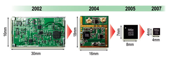
The RF front-end tends to have a high number of surface-mount components. Currently, this has been reduced to only a few components, down from more than 100 only a few years ago. For instance, note that the form factor of the RF PA has shrunk considerably over the past few years (see Figure 4). Area has tended to shrink by a factor of 2 or more each year, with the latest PAs measuring at about 4 mm2. Increased integration has allowed wireless RF to proliferate in consumer electronics, including printers, cameras and mobile phones. But this level of integration is simply not enough. What the industry really needs is a complete, pretested, plug-and-play RF functional block that can be effectively dropped onto a motherboard.
However, in RF designs, monolithic integration needs to be carefully considered in terms of trade-offs to performance and power consumption. To balance these concerns, many of the latest wireless designs are incorporating RF system in package (SIP) technology, which brings together the best processes for different RF front end functionalities, optimizes system performance and houses it all in a single package. SIP designs tend to have the best balance of low cost, high performance and power consumption. In addition, RF front ends in a SIP configuration are simple 50 ohm in/out, allowing ease of system integration.
Optimized Building Blocks
In a SIP design, each block is optimized for cost versus performance (see Figure 5). By creating standard building blocks, SIP designers can quickly customize a design for a particular application or customer. SIPs also offer the advantage of a laminate substrate, which can be used for routing and the inclusion of surface-mount components within the package. The substrate also allows designers to make small changes/adjustments to optimize performance for each customer, a type of mass customization. By developing pre-validated RF building blocks, SIP designers can include them in different modules, providing a validated design in one third to one quarter the time it takes to spin an IC.
For example, Figure 5 shows a dual-chain RF front-end module (FEM) for 802.11 a/b/g/n designs where designers were able to choose a specific technology for each block in order to optimize performance. For instance, the 5 GHz PA is GaAs HBT, the dual-band LNA and switch are GaAS HEMT, the filters are implemented in a passive component only process, and the 2.4 GHz PA and logic are integrated in BiCMOS. In this type of application, the SIP approach allows a mix of technologies in a single package, allowing system designers to choose the best technologies and then do a module integration to deliver all of the functions that a customer wants in a short time. The advantage here is a single package with the RF front end functionality that can be dropped into a design to add wireless capability.
Available Technologies
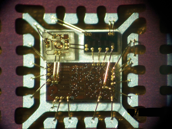
Despite its many advantages, the use of a laminate substrate in SIP designs affects package height, assembly complexity and cost, so package and assembly are becoming important areas of research. One recent trend is toward the use of multi-die QFN. Figure 6 shows a multi-die 3x3 mm QFN that achieves the < 0.5 mm height required for mobile phones. The innovative package shown here also includes a number of thru-die vias, which are critical to reducing size and the number of required wire bonds.
In the latest state-of-the-art smartphones, the RF signal chain requires a surprising 18 mm2 of board space. In Figure 7, the RF chain is the area surrounded by the dotted line. Note the large footprint also required for voltage regulators and enable functions. The addition of WLAN in mobile handsets is driving a need to integrate all of these components into a 3x3 mm package.

To address this need, some designers using GaAs for power amplification are achieving good integration of the PA with low-noise amplifiers (LNA) and switches. These multi-function RFICs have only become available recently, and foundry support for fables RF design companies planning to use these technologies is still not mature. TriQuint Semiconductor recently announced GaAs RFICs for the front-end with this level of integration. However, because it is implemented in GaAs, the device still requires external filtering and control circuitry that needs to be implemented in silicon. In addition, since the designs are transistor-based, they cannot integrate CMOS-based control logic.
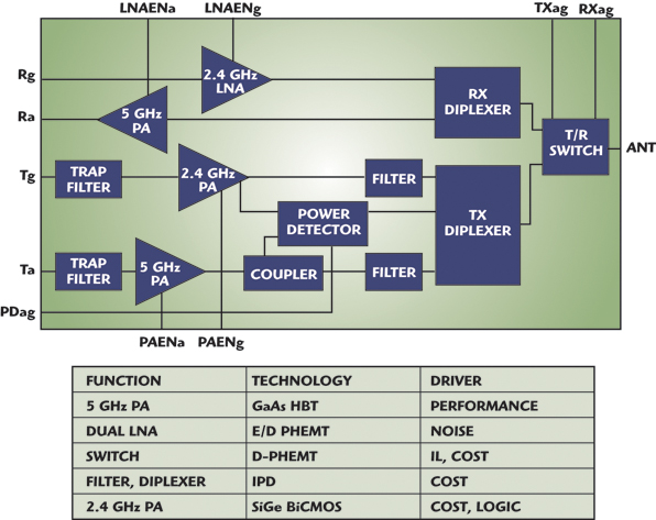
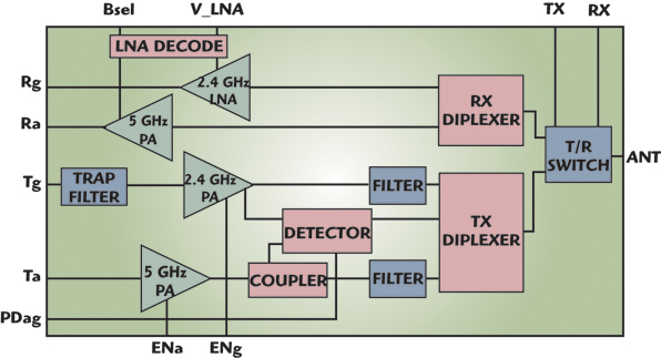
Taking the RF functionality to the next level of integration requires the use of BiCMOS to address the addition of control logic. As a result, the integration of SiGe bipolar RF performance with SiGe CMOS bias-and-control functionality onto a single, small-footprint integrated circuit is a key enabler for the rapid growth of wireless connectivity for multimedia services in mobile consumer electronics devices. The next generation front end modules (FEM) under development integrate multiple power amplifiers, LNAs, power detectors, a T/R switch, filters, diplexers and associated matching circuitry (see Figure 8). This type of module can operate directly off of the battery, which removes the need for external regulators, as required in GaAs RFICs.
During all of this advanced integration, coexistence filtering will also be of paramount importance. To be successful, the RF signal chains required for Bluetooth, WiMAX, FM radio, Wi-Fi, NFC and GPS services cannot interfere with each other. Of great concern will be Wi-Fi and CDMA because of their close proximity to each other, so module and RFIC designers will need to be especially careful with filtering. When logic can be implemented in the module/chip, programmable filters can be used to alleviate coexistence issues, and each function can be fully optimized. This programmability will allow tighter production controls as well, giving OEMs a more uniform product.
Some SiGe BiCMOS products are already available in flip-chip chip scale packaging (CSP). Most wireless connectivity modules, including the transceiver and RF front end, are all trending toward flip-chip architectures because of the low cost of assembly. In addition, flip-chip CSP offers the smallest footprint, lowest height solution, making it very desirable for portable wireless applications. Another advantage of BiCMOS is that there are mature foundry services available for manufacturing in high-volume, low-cost production quantities, and the world’s big foundries all have well-established roadmaps that are based on BiCMOS.
Future Developments
With the drive toward BiCMOS integration, the future of the RF signal chain will likely see a serial interface, which will also allow designers to reconfigure PAs on the fly as part of the power control loop to address the needs of emerging multi-band, multi-standard wireless designs. For example, if you want to have Wi-Fi operate at a low power level, with a serial interface you can reconfigure the PA depending on the local power level required. Currently, this is done by simply backing off power, which negatively impacts efficiency. You will be able to optimize efficiency, which is particularly important for next-generation OFDM designs.
For designers, there is also a well-established roadmap for involving BiCMOS technology nodes and integrating pre-validated standard blocks. So, with BiCMOS, instead of designing transistors for customized functionality, engineers can pull and license intellectual property (IP) blocks for standard functions or trade them between development groups within a company. This allows companies to focus their limited design resources on supporting customers and speeding time to market.
Most designers recognize the advantages of silicon CMOS, and many see SiGe as the natural bridge technology to silicon. In the end, BiCMOS technology uniquely combines the strengths of HBTs (PA, LNA, RF switch) and CMOS (bias and control) in a single manufacturing process.
As a result of a transition to BiCMOS technology and plug and play RF functionality, we can expect RF to be the third wave of the fabless design revolution, following in the successful tradition of digital CMOS and high-speed analog design. At the highest level, the future of wireless is simple: making the world a smaller place. In 2007, social networking became the largest contributor to Internet traffic,2 and we can expect this trend to migrate to mobile devices. Wireless provides human beings with personal interaction and access to information and entertainment in ways no other technology can provide—on-demand, anytime, anywhere, in any format. And people who interact with each other, who share access to information and entertainment with each other, tend to be people who enjoy each other. This is indeed a great model for the future of wireless.
References
1. D. Poulin and G. Rabjohn, “Raising the Bar for the Radio: Making 802.11n Work,” EE Times, January 14, 2008, http://www.eetimes.com/.
2 C. Duffy Marsan, “How MySpace is Hurting Your Network,” Network World, http://www.pcworld.com/businesscenter/article/133494/, May 13, 2008.

John Brewer, Jr.’s 25 years in the wireless semiconductor industry extend across the disciplines of engineering, marketing and management at the senior executive level. Prior to joining SiGe Semiconductor, he was CEO and president of Xindium, a company providing RF power amplifiers for next-generation mobile handsets and terminals. Previously, he founded Vincio, a marketing consultancy. Brewer was also a founder and vice president, marketing of Tropian, a company that developed a revolutionary approach to cell phone front ends. Over the years he has successfully grown wireless transceiver product lines in management positions at SEIKO Communications, Analog Devices and Tektronix. He holds a BS degree in electrical engineering from Santa Clara University.

Peter L. Gammel has worked with single-electron devices, superconducting devices, and MEMS and RF acoustic wave devices for more than 20 years. He is well acquainted with the processes of intellectual property investment, new product and funding development. Gammel previously served as VP engineering at a venture-backed startup. He was chief technology officer at both Advance Nanotech Inc. and Agere Systems, and was a research director at Bell Laboratories. He has more than 200 referred technical publications and more than 25 patents issued and in process. He holds a PhD degree in physics from Cornell University and BS degrees in physics and mathematics from the Massachusetts Institute of Technology (MIT).