

The current drive for increased bandwidth will ultimately pressure the wireless community to exploit higher operational frequencies beyond 20 GHz. A major obstacle associated with high frequency operation is signal distortion which can be the result of nonlinear effects, typically introduced by active devices. Signal distortion resides on the forefront of each engineer’s mind and must be accounted for. The distortion can be compensated by using complex linearizing circuits or simply accounted for in the link budget as a power penalty. This penalty will adversely affect the overall communication system efficiency, resulting in higher operational costs over the lifetime of the system. Many designers will go to great lengths to maximize the reliability of a design and minimize complexity, which eventually prompted the birth of a passive temperature compensation solution for amplifiers.
Market available GaAs- and GaN-based amplifiers specified past 20 GHz tend to be very temperamental with respect to changes in operational temperature. Generally speaking, transistor gain (β) decreases with increasing temperature. This effect is self-compounding considering transistors are not 100 percent efficient and dissipate power as heat resulting in further heating and reduced gain.
Designs do exist where temperature variation is not that important; however, this is not the norm. Temperature induced gain variations must be considered for a majority of designs and are usually corrected by employing either passive or active compensation techniques. Active compensation is flexible and can be advantageous in some applications; however, this flexibility comes with a hefty price tag in performance related drawbacks, such as distortion introduction, system complexity and overall MTBF. The shortcomings of active compensation can be addressed with an enhanced passive solution, which allows more temp-comp flexibility than previously available passive products while operating up to 40 GHz. The challenge is to provide enough passive temperature compensation to ensure stable, temperature invariant outputs from—55° to 125°C.
Passive Temp Comp History
Traditional passive temperature compensation techniques employ chip thermistors that respond quickly to changes in operating temperature. Thermistors are simply resistive elements with a predetermined temperature coefficient of resistance, usually specified in ppm, for linear temperature characteristics or β for exponential temperature characteristics. Either a single chip thermistor or a plurality of chip thermistors configured in a distributed PI or TEE structure can be used for temperature compensation requirements (see Figure 1). This plurality of thermistors is comprised of thermistors with temperature coefficients that can be either positive or negative (PTC or NTC) and integrated into a single chip to provide optimum RF characteristics.

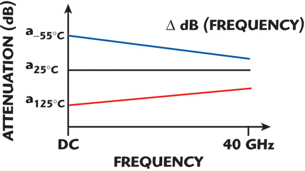
In a world where parasitics do not exist, the transfer function of a temperature variable attenuator (TVA) would follow the behavior exhibited in Figure 2, which is a flat set of attenuation curves for three temperature points from DC to 40 GHz. With α–55C, α25C, α125C being attenuation at –55°, 25° and 125°C, respectively.
Ideally, the TVA will approach 0 dB at 125°C to minimize system loss. Due to this requirement, a figure of merit is used to quantify the normalized amount of temperature compensation, which is referred to as temperature coefficient of attenuation (TCA). TCA is used as a measure of compensation amount for a given nominal attenuation. TCA is determined by linear regression to calculate the best fit slope of attenuation vs. temperature and normalizing to nominal 25°C attenuation. The governing expression for TCA is:
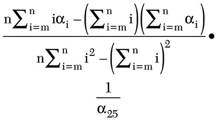
where
αi = attenuation in dB at “i”
degrees C
αi = α–55, α–35, α–15, α5, α25, α45, α65, α85, α105, α125
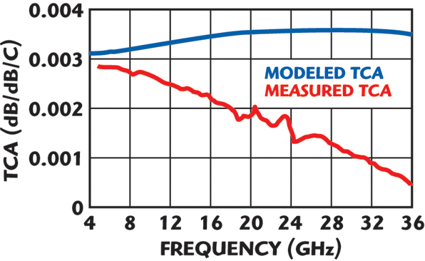
During the manufacture of a TVA to be used in the GHz frequency range, ideal material properties, processing constraints and parasitic reactance come into play affecting the overall performance of the device. The end result of such non-ideal behavior can result in compression of temperature compensation as the operating frequency increases. The TCA becomes a function of frequency. This phenomenon is acceptable for many applications since the TCA frequency compression is a known, predictable quantity. An example of TCA compression can be seen in Figure 3 and the corresponding TCA is plotted in Figure 4 as a function of frequency.

For applications requiring significant temperature compensation well into the GHz range, several TVAs are required to fully compensate a system. Referring to Figure 3, a 40 GHz application would require three times the number of TVAs as a 1 GHz application. This scenario also would introduce three times the nominal loss at 40 GHz. This exemplifies the need for a passive temperature compensation technique to improve TCA performance beyond 20 GHz.
Performance Modeling, Correlation and Compensation

The high price of gain beyond 20 GHz is placing demands for more temperature compensation with less loss penalty, which is effectively a greater TCA. Creating accurate electromagnetic (EM) models in the design phase is critical when attempting to shorten the design cycle. Planar EM simulators can aid in the prediction of RF parasitics and discontinuities; however, some parameters can not be accounted for in the model and must be synthesized empirically.
To empirically develop an enhanced EM model, it is imperative to compare simulated performance versus actual measured data. This comparison provides a significant amount of information for analysis and can be seen in Figure 5. The corresponding TCAs as a function of frequency are plotted in Figure 6 to help demonstrate the difference between expected performance across temperature and frequency and actual measured data. From the plot it is easy to see the measured data undergoes a TCA compression of approximately 80 percent from 4 to 36 GHz.
Having both predicted and measured data available, the original model can be modified to account for measurement discrepancies. This new model, referred to as the “enhanced model,” can be utilized to more accurately predict the TVA performance. For example, analysis of the measured response in Figure 5 shows the transfer function of the attenuator begins to have mild, high-pass characteristics at the low temperature extreme. These characteristics appear due to stray, parallel capacitance across the series element of the attenuator network, as seen in Figure 7, not to mention other random variables that contribute to this temperature dependant capacitance. This is the reason for an empirical solution versus and analytical approach.
Adjusting the model to account for this temperature induced, capacitive event requires the addition of lumped-element, reactive components to the original model. With the information obtained in the comparative analysis, the correlation factors (reactance values) are fed back to the original TVA model. This feedback results in a correlated, “enhanced model” which now can be used for design optimization for specific TVA requirements.
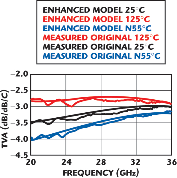
Adjusting the amount of reactance in the model at each temperature is adequate to provide a correlated model to be used for TVA synthesis. For example, the model used in the simulation to create the data in Figure 5 was adjusted with the correlation factors empirically derived by the comparative analysis between the simulated and measured performance. This “enhanced model” was then re-simulated. The enhanced simulation data is superimposed on the original measurements and can be seen in Figure 8.
Most Ka-band temperature compensation requirements are for the greatest TCA with the lowest nominal attenuation. Communication channels operating at Ka-band are generally upconverted signals having a small percent bandwidth. Because the bandwidth requirements are narrow, compensating the previously defined enhanced model can be accomplished by the introduction of a reactive tuning structure. As with any RF tuning, this technique will introduce frequency selection into the TVA design and ultimately limit the bandwidth of the TVA. This technique will mitigate the high-pass filtering effect.
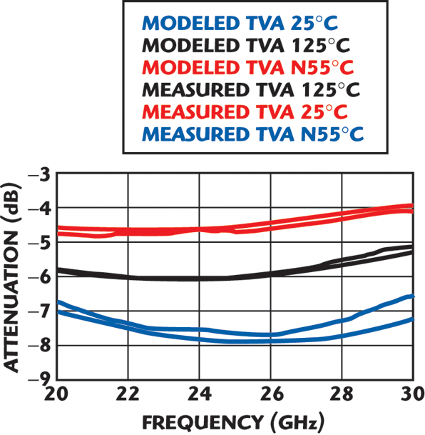
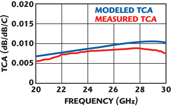
Compensating the enhanced model to meet specific temperature compensation requirements can be accommodated by fabricating distributed reactance’s on the same chip as the TVA. This allows a compact, single chip temperature compensation with a TCA as high as –0.010 dB/dB/C. The technique is currently proven out to 40 GHz, with approximately 2 GHz of bandwidth. A compensated TVA model along with the corresponding measured data can be seen in Figure 9 with the TCA of each depicted in Figure 10. This showcases EMC Technology’s ability to accurately predict TVA performance, thus reducing the overall development cycle for RF temperature compensation.
Conclusion
Enhancements in modeling and measuring temperature variable attenuators has reduced the product design cycle. This has enabled EMC Technology to address current temperature compensation requirements that were once considered beyond the technology. The flexibility and reliability of this proven technology has paved a way for passive temp comp to be the choice for designers developing products operating as high as Ka-band.
Florida RF Labs/EMC Technology
Stuart, FL
(800) 544-5594
www.rflabs.com
RS No. 303