
For many years Southwest Microwave has manufactured field replaceable connectors and launch accessories where connector performance was easily verified by measuring two connectors back-to-back as a two-port device. The responsibility for packaging and board layout fell to the user to develop independently.
With the introduction and success of Southwest Microwave end launch connectors, the packaging responsibility has fallen to Southwest Microwave; the user is now only responsible for board layouts. To assure maximum performance of the Southwest Microwave end launch connectors, equally high performance test boards were needed to accurately measure the connectors.
In the pursuit of high performance test boards, it was decided to broaden the research project and begin a comprehensive study of board layout design variables and their effects on microwave performance. This evaluation on 30 mil Rogers 4350 material explores transitions of grounded coplanar waveguide (GCPWG) and microstrip lines to coaxial connectors with the use of Southwest Microwave end launch connectors. The baseline for the GCPWG portion of this study is an older board design that worked reasonably well to 45 GHz. The use of 3-D simulation was included in this evaluation.
End Launch Connectors
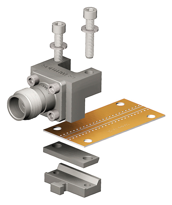
The connectors used are Southwest Microwave end launch connector assemblies, model number 1492-02A-5 (see Figure 1). These connectors were designed for single-layer and multi-layer boards where the top layer is the microwave layer. The 1492-02A-5 has a 2.4 mm female connector and a transition block with a 10 mil diameter circuit launch pin and a 63.5 mil diameter coaxial ground. Because they were for multi-layer boards, there is a 20 mil overhang of the ground over the board to catch the top ground of the board which is useful for single-layer GCPWG.
No soldering is needed to connect the end launch connectors to a board due to a slight interference fit between the circuit pin and the board to ensure good contact. This means that the connector can be re-used. All of the data in this study (over 30 boards) was taken with the same two connectors.
Test Equipment and Techniques
An Agilent 8510D network analyzer was used for all of the published measurements. The test port connectors used were 2.4 mm connectors and the frequency range for all measurements was DC to 50 GHz. Calibration was a full 12-term SOLT calibration with sliding loads. The TDR measurements were set up as low pass step in real units. All of the data was taken from the same calibration. Some internal verification of data was done on an Anritsu 37297 network analyzer.
Review of Original Test Board (2003)
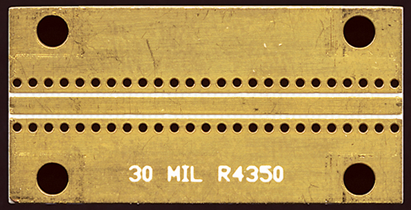
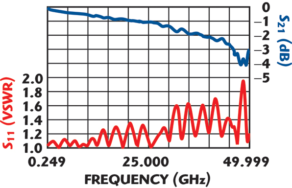
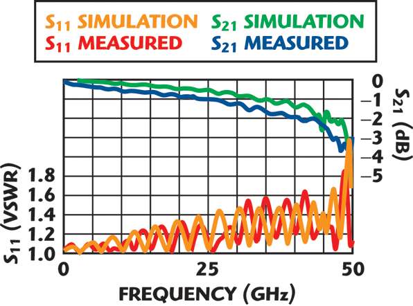
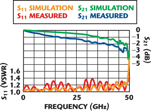
When the end launch connectors were first introduced in 2003, a one-inch long GCPWG test board was developed for testing (see Figure 2). One of these original test boards was used in this study to establish the baseline performance of the connectors. The results of the original end launch connector test board, displayed in Figure 3, shows a glitch in the loss starting at 45 GHz that is characteristic of this board.
3-D Simulation of the Original Test Board
CST MWS Model
3-D simulation models have promise to be useful tools in developing good transitions from coaxial lines to coplanar or microstrip lines. With this hope in mind models were worked out for many of the line structures and some results are shared in this article.
Simulation is used to predict results of these types of structures then changes are made and the results of that change are viewed without having to fabricate and test actual hardware. CST Microwave Studio® (CST MWS) was used for many of the simulations in this study and CST provided the simulations.
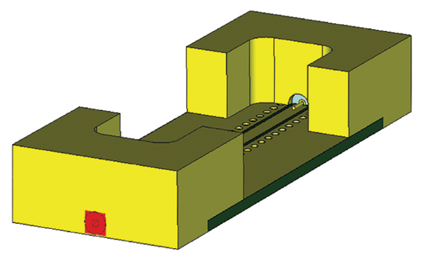
The 3-D simulation model is created by only looking at the transition blocks and the test board; the connectors are not part of the simulation (see Figure 4). The biggest discontinuity in the transmission line is the transition from coax to PCB and the worst transmission line is the PCB itself. The two coaxial connectors are well matched and have very low loss, so even without them in the simulation a very good correlation to the actual performance can be achieved.
Simulation Results
The simulation results displayed in Figure 5 show the insertion loss has a dip at 45 GHz and the VSWR slowly rises over frequency from below 1.2 to 1.6 through 45 GHz. Both of these are characteristic of the test board and show good correlation of simulated to measured.
Understanding the Importance of the Launch to a GCPWG
Determination of the Optimal Launch (Taper)
At the end of the board where the launch from the board’s microwave transmission structure to a coaxial line occurs, there is a pin from the coax sitting on top of the board. This added metal creates an increase in capacitance that has to be addressed for optimal performance. The way to compensate for the capacitance of the pin is to add inductance to the board. This can be done in both microstrip and GCPWG by narrowing the trace. The method used here is reducing the trace in what is referred to as a taper.
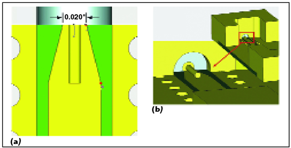
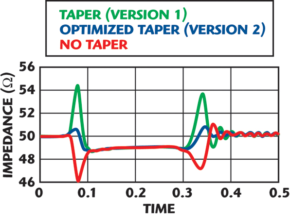
This is the first study by Southwest Microwave where the taper of GCPWG is examined in detail. The traditional way a taper was determined was to match the width of the trace with the coax launch pin, then taper it out to the proper microstrip width over the distance that the pin sits on the line (see Figure 6). For the model 1492-02A-5 the through pin is 0.020" so the end of the taper is 0.020" to match it. It has been shown in earlier test boards that this may be over-compensating for the capacitance, so the CST MWS 3-D model was again used to get a prediction. The result of the simulation showed this taper makes the launch inductive and the performance is actually worse than having no taper at all (see Figure 7).
Optimized Taper (Version 2)
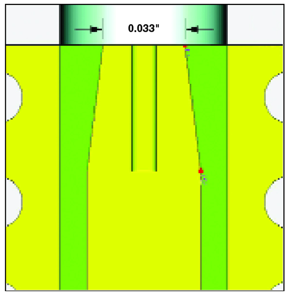
The second taper design, shown in Figure 8, was developed using CST Microwave Studio’s optimization routine. The taper length was kept the same, but the final dimension at the edge of the board was the variable in the optimization and it was increased to 0.033". This still adds some inductance to the board right at the launch, but it is less inductive than the first taper design. The simulation and actual data show improved results for S11 and the insertion loss is very smooth up to the normal 45 GHz glitch always seen (see Figure 9).
Improving Bandwidth: Mystery of the Vias
After optimizing the match, the bandwidth was studied. It has been assumed the vias played a role in bandwidth, but there was no clear explanation of what that role was exactly.
Channelized Coplanar Waveguide
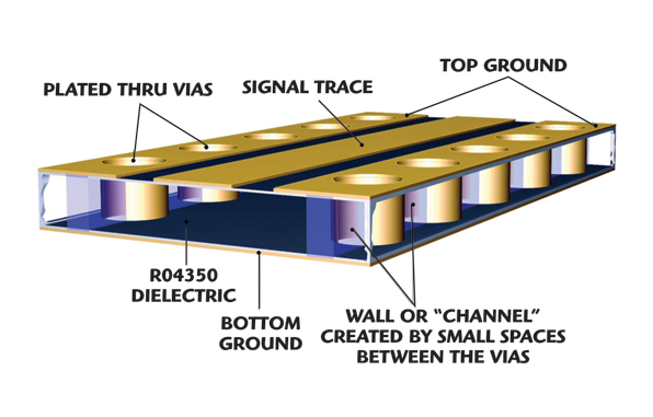
While doing research into proper via placement, a reference to channelized coplanar waveguide (CPW)1 was found that explained the function of the vias as it related to bandwidth (see Figure 10). Channelized coplanar waveguide is a GCPWG structure with lateral walls that create another waveguide mode and stops surface wave inside the structure from being created.
Purpose of the Vias
Once it was determined that placing lateral walls would increase the bandwidth of the circuit and that the vias were acting as a microwave wall, the spacing of the vias became more predictable. In general, microwave energy will reflect from openings less than a quarter wavelength of the signal.
The other determining factor in the high frequency performance of the vias is the spacing between the rows of the vias. The wider the spacing, the lower the cut-off frequency and the closer the spacing the higher the cut-off frequency.
Realization of Lateral Walls by Closely Spaced Vias
The illustration in Figure 10 shows the GCPWG used for these test boards. Rows of plated through vias are used to tie the top ground planes to the bottom ground plane, simulating a wall as shown in shadow between the vias. Microwave energy will not pass through spaces that are less than a quarter wavelength of the frequency, so the spacing between the vias becomes the critical dimension.
Analysis of Spacing Between Vias
The original test board shows the VSWR gently increasing over frequency through 50 GHz. This increase in VSWR is due to the match and as seen in the previous section can be addressed by introducing a taper at the launch.
The insertion loss is fairly smooth until 45 GHz. The reason for the glitch at 45 GHz is a function of the vias. The original test board has 25 vias of 0.020" in diameter and equally spaced at 0.040" centers. Since the purpose of the vias is to create a “wall,” the important dimension of the vias is the space between the vias, or the dimension from the edge of one via to the edge of the next via. For this board the spacing is 0.029", which in RO4350 with a dielectric constant of 3.66 corresponds to a quarter wavelength frequency of 53 GHz. The via rows spacing is 0.112" and is also a determinant in the performance of the board. Again, closer spacing should lead to higher frequency operation.
To test this theory a series of additional boards with 3, 7 and 13 vias were made and tested. With only 3 vias on a one-inch board, the spacing between the vias is 0.460". The quarter wavelength frequency in RO4350 is 3 GHz. The board operates without any glitches to 5 GHz, so there is some correlation shown.
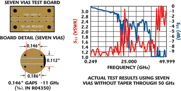
With seven vias on a one-inch board, the spacing between the vias is 0.146" (see Figure 11). The quarter wavelength frequency in RO4350 is 11 GHz. The board operates without any glitches to 13 GHz, so there is more correlation shown and a clear improvement as the vias are added and the spacing between the vias is decreased.
With 13 vias on a one-inch board, the spacing between the vias is 0.0683". The quarter wavelength frequency in RO4350 is 23 GHz. The board operates without any drastic glitches to 35 GHz, so there is even more correlation shown and a clear improvement as vias are added and the spacing between the vias is decreased.
Analysis of Spacing Between Via Rows
It has been seen in the previous boards that they will work somewhat above the quarter wavelength frequency, so the original board has a via space corresponding to 53 GHz and it should work easily to 50 GHz. There is still the glitch at 45 GHz, so there must be some other factor involved.
It has been speculated that making the rows closer will increase the bandwidth of the board. To determine the effect of the row spacing a board was made where the rows were moved out to 0.126" from the original 0.112". The first glitch in insertion loss moved to below 40 GHz so a wider spacing does show a degradation in performance.
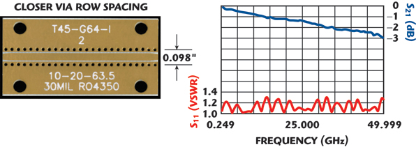
The original test board had a spacing from the centers of the rows of 0.112". A reduction of this spacing should increase the frequency response of the board. A distance of 0.098" was chosen as it was the closest spacing to the coplanar structure that could be achieved in normal board manufacturing processes.
The data from the test board with a 0.098" spacing, shown in Figure 12, confirms the increased bandwidth of the board and the loss curve is smooth through 50 GHz. This final result shows that GCPWG can create boards with much higher frequency performance than what microstrip may be limited to on the same material.
Conclusion
This study was conducted by Southwest Microwave to evaluate grounded coplanar waveguide (GCPWG) launches and lines, top ground (coplanar) launches to microstrip lines, and microstrip lines running straight to the edge of the board on 30 mil Rogers 4350 boards. This article only includes the material related to GCPWG and has shown how to improve match and bandwidth on GCPWG. Hopefully this study, the complete version of which includes microstrip lines and an analysis of loss, has been helpful to board designers working at microwave frequencies to have a better understanding of launch and transmission line structures. Contact Southwest Microwave for more information.
Acknowledgments
The mechanics of the layouts were done by a consultant (Petra Microwave) and the boards were fabricated by Accurate Circuit Engineering in Southern California. The material was supplied as samples by Petra Microwave® Ltd., Rogers Corp.,® CST®-Computer Simulation Technology and CST Microwave Studio® 2006. All are registered trademarks of their respective companies.
References
1. R.N. Simons, Coplanar Waveguide Circuits, Components and Systems, Wiley-Interscience, John Wiley & Sons Inc., New York, NY, 2001.
2. B. Rosas, “50 GHz End Launch Connector Test Boards: The Description of the Development of Coax to Grounded Coplanar Launches and Through Lines on 30 mil Rogers 4350 Material with Comparison to Microstrip,” DesignCon 2008.
Bill Rosa holds his BSEE degree from Arizona State University, specializing in microwaves, and his MBA degree from the University of Phoenix. He is the product engineering manager at Southwest Microwave, responsible for engineering on all standard interface connector products. He joined the company in 2003 as a senior product sales specialist. While in that position he became the acting product manager for the end launch connector product line. Creating test methods for end launch connectors led him to this ongoing study of launch structures and transmission lines. He has 15 years of experience in the microwave industry, including applications engineering positions at Rogers Corp. (high frequency capacitors) and Giga-tronics (test equipment).