
Achieving high linearity while preserving high efficiency in a power amplifier is a real design challenge. A few approaches have been reported to achieve good linearity and high efficiency in a power amplifier. These techniques use envelope tracking of the input voltage and adaptive bias methods. Hanington, et al.1 achieved an ACPR greater than 26 dB with a dynamic power supply voltage for CDMA. Anderson, et al.2 have demonstrated an efficiency increase from 20 to 32 percent for CDMA IS‑95 using the envelope tracking method. With an adaptive bias technique, Noh, et al.3 showed an ACPR improvement of 4 dB with a deep pinch-off bias.
In this article, an adaptive bias technique is proposed to meet the high linearity requirements of the high degree digital modulation standard. The adaptive bias technique is investigated to improve both linearity and efficiency of the power amplifier. The optimal device loading impedances and the design of the matching networks are studied for wide bandwidth applications. A prototype power amplifier is demonstrated with an output power of 34 dBm at the 1 dB compression point, an ACPR of –37 to –38 dBc and an efficiency of 35 to 37 percent in the 800 to 900 MHz frequency range. The power amplifier prototype was extended with a Cartesian feedback IC and an overall ACPR performance from –65 to –67 dBc was measured.
Principle of Operation

Adaptive Bias Technique
The adaptive bias technique allows the change of the quiescent current of a device with respect to the input power level, meaning that a low quiescent current at low output power level and an increasing quiescent current at high output power can be achieved. This technique simultaneously provides both high linearity and efficiency characteristics over a broad range of power levels.2 For multistage amplifiers, similar techniques can be employed for each stage of the amplifier. This can give high gain, high output power and high efficiency at the same time. Each stage of the amplifier operates in deep class AB at fairly low quiescent current. As soon as the input power is applied to the amplifier, the bias point is shifted to produce optimum power performance. Figure 1 shows a single-stage power amplifier utilizing an adaptive bias technique.
Bandwidth Analysis
The inherent bandwidth (BW)i is the bandwidth obtained under conjugate matching conditions, where the matching loads terminate the two-port device. A conjugate match means that Γs = Γ*N or Ys = Y* and YIN, where Γs and ΓIN are the reflection coefficients of the matching network and the device, respectively. Ys and YIN are the corresponding admittances. The inherent bandwidth is given by

where f0 is the frequency where the conjugate match values were obtained and Q is the quality factor of the parallel network defined by

By substituting Equation 2 into Equation 1, one can express the inherent bandwidth as

where
R = 1/2G
|B| = ω0C = 1/ω0L

From Equation 1, to achieve a wide bandwidth, the Q of the network has to be low enough. Similarly from Equation 3, it should be noted that the conductance G must be high enough, while keeping the susceptance B at a low level in order to maximize the bandwidth.
Cartesian Feedback
A Cartesian feedback generates high output power signals with good ACPR. This is accomplished by coupling off a part of the demodulated signal to pre-distort the input baseband I and Q signals, via a comparator circuit.4 The block diagram of the Cartesian feedback architecture is shown in Figure 2. The modulated signals are considered as a sum
A(t)sin(ω0t + Φ(t)) =
I(t)sinω0t + Q(t)cosω0t (4)
I(t) = A(t)cosΦ(t) (5)
Q(t) = A(t)sinΦ(t) (6)
The demodulated signals of Cartesian feedback can be expressed as
I' = (Isinωt + Qcosωt)sin(ωt + Φ) (7)
Q' = (Isinωt + Qcosωt)cos(ωt + Φ) (8)
where ω is the carrier frequency.
Design Example Using a GaAs HBT Power Amplifier

The goal for the power amplifier is to achieve an ACPR of 35 dBc at an operating power of 30 dBm in the frequency range of 800 to 900 MHz. The device used in the three-stage power amplifier is the RF21735 transistor from RF Micro Devices, which has been found suitable for the present task. It offers an operating gain of 32 dB and is manufactured in an advanced gallium arsenide heterojunction bipolar transistor (GaAs HBT) process technology. In order to keep the junction temperature within a margin below the specifications, an obligatory power-added efficiency (PAE) higher than 30 percent was calculated for an operating power of 30 dBm.
The device utilizes an adaptive bias scheme. A low gate voltage is applied to the device, which provides a deep class AB bias, keeping the quiescent current at a low level. A broadband matching network with a loaded Q of 5 is chosen to transform the optimum load impedance ZOL to the 50 Ω load termination. The load impedance is obtained from a simulation template and correlated with the measurement data. A three-stage, low-pass matching network is used to transform the optimum load impedance to 50 Ω. The first matching component is a tapered microstrip line, which significantly increases the efficiency for a wide frequency band.

A second harmonic trap is introduced in the final stage feeding line. The bonding wires together with the external capacitor form a series resonator that should be tuned to the second harmonic frequency in order to increase the efficiency and reduce spurious output. The grounding of each stage is essential and must be directly connected to the ground plane by vias under the device. A short path is required to obtain optimum performance as well as to provide good thermal dissipation.
Measurement Results
A test board using FR-4 material was fabricated. The printed circuit board (PCB) has a dielectric of 4.5 and a thickness of 14 mils. The test board is shown in Figure 3. The test board size is 40 x 30 mm. Experimental studies show that a 200 μF tantalum capacitor (POSCAPS model from Sanyo) is required at the supply line to improve the transient ACPR due to switching and wide band noise. When changing the power level from noise power to steady-state power, the transient ACPR due to switching depends upon the switching time.
Typically, in digital modulation, the input RF (I and Q baseband signals) will provide the control of the switching time. Nevertheless, the common practice to identify the problem is by observing the peak-to-peak ripple of supply voltage. The high-speed Agilent 1 GHz oscilloscope (4GSa/s) 54832B DSO is used to measure the ripple voltage. In the prototype board, the peak-to-peak ripple of supply voltage is approximately 180 mV. High Q capacitors (from AVX) are used for matching networks.
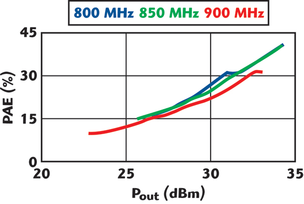
For the 1 dB compression point and efficiency characterizations, a gate bias with a duty cycle of 25 percent and a pulse width of 600 μs is applied. The ACPR parameter is measured with an IfR 2310 Digital Modulation Analyzer. A π/4QPSK modulation is used to measure the ACPR parameter. A current probe with a Tektronix scope was used to measure the DC current. The measured power at saturation, 1 dB compression point, gain at the rated power, PAE and ACPR are shown in Figures 4 to 6, respectively.
To measure the closed loop ACPR performance, a Cartesian feedback IC is used. The amplifier test board is used with a Cartesian feedback IC provided by Motorola. An additional ACPR value of 30 dBc is obtained at ±25 kHz with the closed loop performance. Measurement results of the closed loop ACPR across the bandwidth (800 to 900 MHz) are shown in Figure 7. The ACPR results are plotted for frequency spacings of ±25 to ±512 kHz. The ACPR performance are within the π/4QPSK modulation specifications.

With the improvement in ACPR, the power amplifier is classified as a more linear device and is applicable to most of the wireless communications. Consequently, a power amplifier with good efficiency as well as good linearity has been designed with the aid of a Cartesian feedback.
Conclusion
This article explains how to achieve a high degree of linearity to fulfill digital modulation (π/4QPSK) standard requirements. A high linearity and high efficiency UHF RF power amplifier, with a wide bandwidth, is presented using an adaptive bias technique. The bandwidth analysis and wide bandwidth matching networks of the power amplifier are discussed. An output power of 34 dBm at the 1 dB power compression point, an ACPR of –37 to –38 dBc and a PAE of 35 to 37 percent for the frequency range of 800 to 900 MHz are measured on an open loop power amplifier. A power amplifier linearization concept, based on a Cartesian feedback, is presented. The concept has been applied for the digital modulation (π/4QPSK) standard in the 800 to 900 MHz frequency range. For the closed loop amplifier with a Cartesian feedback IC, an ACPR of –65 to –67 dBc has been demonstrated on a prototype board. The power amplifier with Cartesian feedback fulfills the digital modulation (π/4QPSK) specifications.

References
1. G. Hanington, P.F. Chen, P.M. Asbeck and L.E. Larson, “High Efficiency Power Amplifier Using Dynamic Power Supply Voltage for CDMA Applications,” IEEE Transactions on Microwave Theory and Techniques, Vol. 47, No. 8, August 1999, pp. 1471–1476.
2. D.R. Anderson and W.H. Cantrell, “High Efficiency High Level Modulator for Use in Dynamic Envelope Tracking CDMA RF Power Amplifiers,” 2001 IEEE MTT-S International Microwave Symposium Digest, Vol. 3, pp. 1509–1512.
3. Y.S. Noh and C.S. Park, “An Intelligent Power Amplifier MMIC Using a New Adaptive Bias Control Circuit for W-CDMA Applications,” IEEE Journal of Solid State Circuits, Vol. 39, No. 6, June 2004, pp. 967–970.
4. B. Razavi, RF Microelectronics, Prentice-Hall Inc., Upper Saddle River, NJ, 1979.
5. RF2173 RF Micro Devices datasheet; Rev A6 030514.