
The development of GaN technology has brought with it the need for accurate nonlinear active device models that can be easily used in standard design tools. A GaN HEMT model should ideally be scalable with gate width and should be able to predict the performance of the device over the anticipated range of frequency, power, bias conditions and temperature.
This article describes the process used to extract such a model for the Nitronex GaN-on-silicon HFET fabricated using the NRF1 process.1
The procedure is generally applicable to a wide range of transistors, but the results may not apply to devices fabricated by other processes, including those in GaN.
A variety of transistor models, both proprietary and public, are available. In the present case, a public model was sought, for which information existed in the literature, was available in major electronic design automation (EDA) platforms and could ideally be ported from one design platform to another with minimal changes.
Also, due to the anticipated usage of these devices in nonlinear applications, it was important to use a model that had minimal numerical convergence issues and was well behaved when used in a harmonic-balance environment.
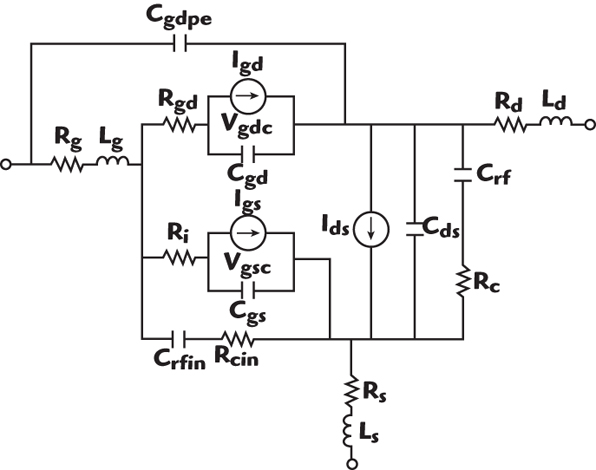
The Angelov2 model was able to meet these criteria and was chosen for this effort. The model equivalent circuit is illustrated in Figure 1. This model is available in both Agilent’s Advanced Design System (ADS) and in Applied Wave Research’s Microwave Office (MWO), where it is known as Angelov2C.
The model is based on the work of Angelov and his colleagues at Chalmers University in Sweden.2 It is useable in a wide range of applications, but here the focus is on power amplifiers, since this is how most designers would use this device.
Data Collection
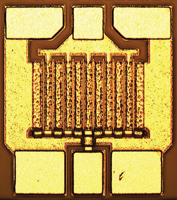
The extraction process started with the choice of a device that is representative of the HEMT process. Although various device sizes were available, the total gate width of the chosen device was 2 mm, composed of ten 200 μm fingers. A photograph of the coplanar waveguide (CPW) probe-able device is shown in Figure 2.
This style of device is included in the production masks of all device sizes in a probe-able configuration. In addition, the current levels obtainable with this gate width are compatible with the limitations of the pulsed I-V test equipment and the device is amenable to accurate S-parameter measurement over a wide frequency range.
First, a production wafer was chosen, which by definition meets all electrical parametric specifications. Sixteen 2 mm devices were diced from a uniform distribution about the wafer and mounted four to a Cu/MoCu/Cu (CPC) package flange. The devices were attached to the flange by a standard AuSi eutectic bonding process.
The criteria used to select the median device from these 16 parts were pulsed I-V at VGS = 0 V curves (pulsed IDSS) and small-signal parameters at 2.14 GHz.
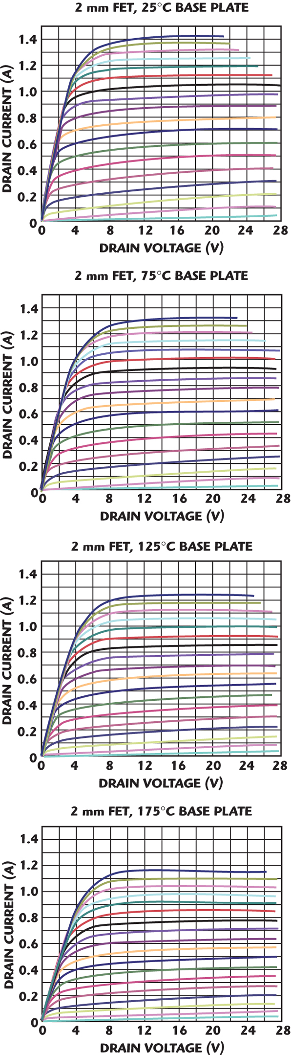
Prior to data collection, the selected 2 mm device was DC biased at 28 V with a drain current calculated to give a junction temperature of 200°C for one hour to provide the effects of burn-in. An Accent DIVA D265 pulsed I-V system was used to collect a family of curves, with the gate biased from –2 to +2 V in 0.2 V steps, and swept from 0 to 48 V on the drain in 0.5 V steps. The source was maintained at ground potential.
The instantaneous power was limited to 30 W. The pulse width was 2 μs, with 2 ms between pulses for a duty cycle of 0.1 percent, which eliminates self-heating.
In addition, to loosely emulate hysteresis effects at RF, the I-V curve data points were collected pulsed from a quiescent point close to a typical operating condition used under RF (VDS = 28 V, Class AB bias).
The pulsed drain characteristics were taken as a function of base plate temperature in increments of 25° from 25° to 175°C. The drain characteristics collected post burn-in and after the entire set of measurements were compared and found to be nearly identical.
Figure 3 shows the IV curve families at 25°, 75°, 125° and 175°C.
Next, S-parameter measurements were collected over a frequency range of 100 MHz to 10 GHz. Since the S-parameter measurement system is not pulsed, there is self-heating, due to the power dissipation at the quiescent operating point. Data was again taken at base plate temperatures, in increments of 25° from 25° to 175°C.

A full set of S-parameters was measured at each bias point with VDS = 7, 28 and 48 V and the gate stepped in increments of 0.1 V, from below pinch-off (VGS = –2 V) to a gate voltage for which the calculated TJ exceeded 200°C.
Model Extraction
Once the I-V and RF data were collected, a subset was used to begin construction of the model. First, a fit was made to the pulsed I-V at a base plate temperature selected to match a typical operating temperature under RF drive (125°C).
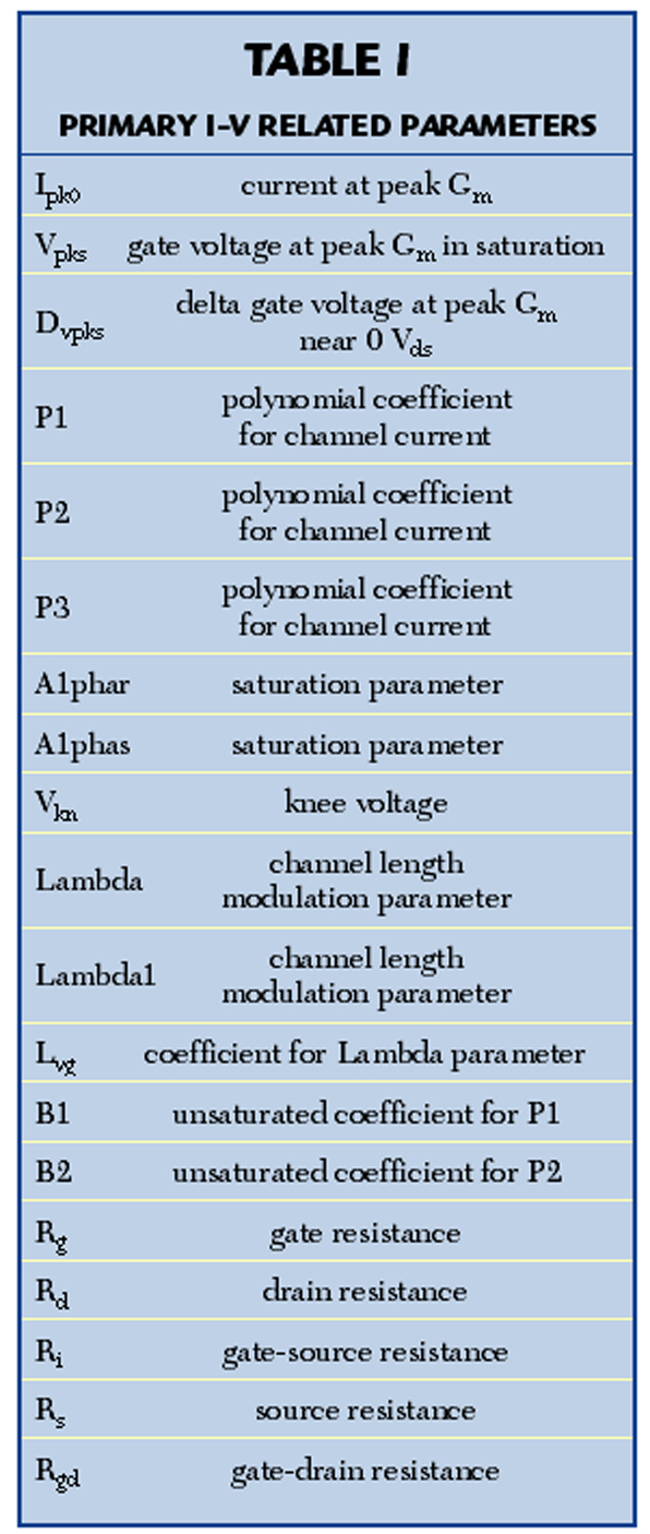
There were approximately 14 parameters and five DC circuit resistor values that needed to be determined at that time. The list of these parameters is given in Table 1.
Once a satisfactory fit was obtained, as demonstrated in Figure 4, S-parameter data at several bias points along the anticipated load line were added to the model project. Three drain voltages were chosen (VDS = 7, 28 and 48 V), with the gate biased sufficiently negative to give a drain current which resulted in approximately 25°C temperature rise due to self-heating.
With the base plate temperature set to 100°C, the self-heating brought the junction temperature to approximately 125°C, which is a typical operating temperature and the temperature of the pulsed I-V used for the fit.
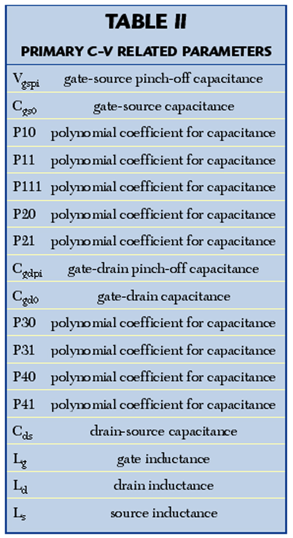
Another 17 primary parameters affect the small-signal fit across the bias. The parameters and their descriptions are tabulated in Table 2.
These fitting parameters were determined using optimization with the I-V parameters fixed. Once a reasonable fit was obtained to the small-signal parameters over the frequency range of 100 MHz to 10 GHz, the model parameters that affect both I-V and the S-parameters were re-optimized.
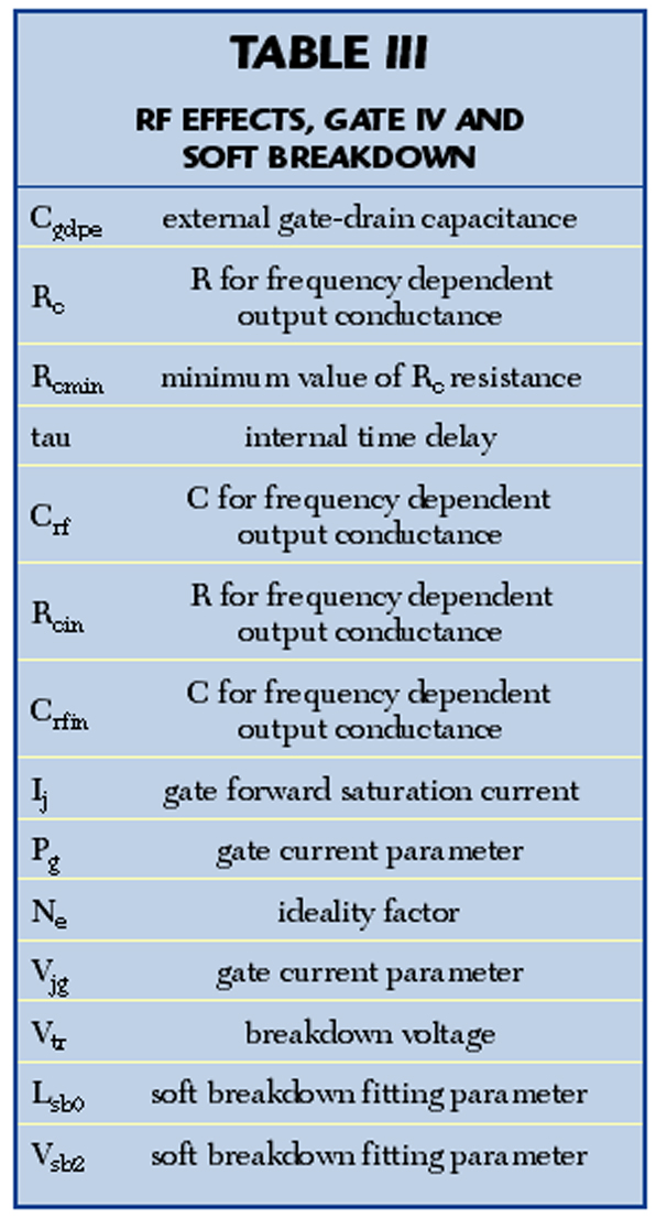
In addition to the primary fitting parameters already mentioned, there are seven parameters specifying secondary circuit elements on the input and output sides of the model equivalent circuit, three parameters are related to the soft breakdown and another four parameters are defining the gate forward characteristics.
All of these parameters are described in Table 3.
The gate diode parameters were fit to the measured data at a 125°C base plate temperature, with special attention to the forward bias region up to a current density of 10 mA/mm.
The gate diode current affects the shape of the drain characteristics as the gate forward bias is increased, resulting in some interplay with the drain I-V fitting parameters that had to be accounted for.
Next, the temperature dependence was incorporated, using two parameters related to the drain voltage fit, three parameters relevant to the S-parameters and a soft breakdown temperature dependence parameter. The fit was made over three temperatures.
A thermal resistance value was provided to allow the model to calculate self-heating based upon the dissipated power.
A thermal capacitance was also specified to provide approximate thermal transient behavior. Table 4 lists all of the temperature related parameters.
Model Validation
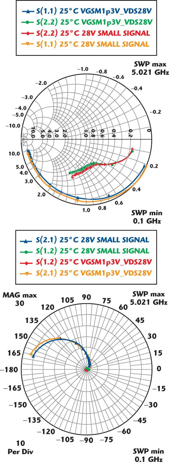
For top-level verification, the model was used to simulate I-V and small-signal RF parameters. Figure 5 shows the measured and modeled S-parameters with S11 and S22 plotted on a Smith chart, and S21 and S12 on a polar chart.
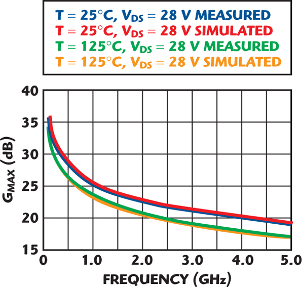
Figure 6 compares the measured and simulated data for the maximum available gain, Gmax, as a function of frequency and temperature.
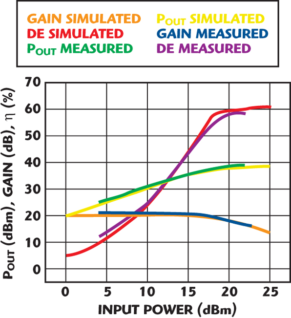
Validation of the large-signal performance is demonstrated by comparison of a simulated load-pull to actual measurements of the 2 mm device. The power sweep data was collected from the device, including output power, gain and drain efficiency, on a standard load-pull system. The frequency was 2.14 GHz and the drain bias was 28 V with the gate biased to give a quiescent drain current of approximately 55 mA.
The input impedance was fixed at a standard value for a 2 mm device testing, and the output impedance was tuned for maximum output power. The input and output impedance values used in the measurements were directly entered into the simulated load-pull.
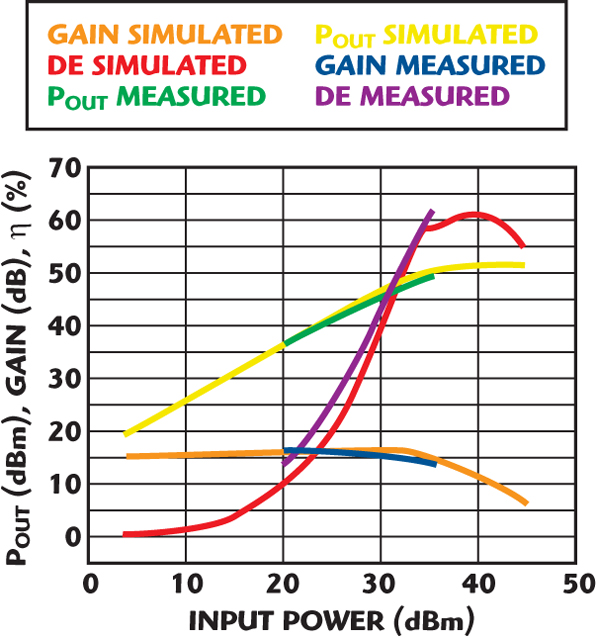
The measured and simulated values are compared in Figure 7. As preparation for delivery as a product model to users, a model for the package and any internal matching circuit are combined with the device model. This simulation is compared to the measured RF performance of packaged devices of various gate peripheries.
One example of such a product is the Nitronex XPT25100. Figure 8 shows the modeled versus measured results for the XPT25100 device. This is a 36 mm gate-width device mounted in an air-cavity package with internal pre-matching on the input side.
Conclusion
The completed Angelov2C-based model has been determined to be robust in terms of convergence under a wide range of conditions. The current-voltage (I-V) output agrees quite well with measurements over the temperature range from 25° to 175°C, from +2 to –2 V on the gate, and 0 to 48 V on the drain.
The small-signal output matches reasonably well from 0.1 to 10 GHz over the typical load line of the device under operation.
The large-signal behavior is predictive and is close to the actual tested device behavior. Self-heating is accurately modeled using a periphery dependent thermal resistance. This device model has been used to provide accurate packaged product models for a number of products and other anticipated device designs.
References
1. J.W. Johnson, J. Gao, K. Lucht, J. Williamson, C. Strautin, J. Riddle, R. Therrien, P. Rajagopal, J.C. Roberts, A. Vescan, J.D. Brown, A. Hanson, S. Singhal, R. Borges, E.L. Piner and K.J. Linthicum “Material, Process and Device Development of GaN-based HFETs on Silicon Substrates,” Electrochemical Society Proceedings 2004-06, p. 405 (2004).
2. Angelov, V. Desmaris, K. Dynefors, P.A. Nilsson, N. Rorsman and H. Zirath, “On the Large-signal Modeling of AlGaN/GaN HEMTs and SiC MESFETs,” 2005 Gallium Arsenide and Other Semiconductor Application Symposium Digest, pp. 309–12.