
Part I of this tutorial article1 gave a detailed discussion and analysis of the start-up and steady-state oscillation conditions for transistor LC oscillators with emphasis on CMOS devices. Part II presents both linear and nonlinear phase noise models for the parallel feedback and negative resistance oscillators. Each approach to the oscillator phase noise calculation has its own advantages and drawbacks. For example, the linear Leeson model for a parallel feedback oscillator expressed in an explicit analytical form is very simple and can explain the dependence of the oscillator phase noise on the resonant circuit loaded quality factor, signal power, active device noise figure and its low frequency flicker noise. However, it is not considering the effect of amplitude-to-phase conversion and higher order harmonics. In this case, the nonlinear Kurokawa model, developed for a negative resistance oscillator, demonstrates the explicit analytical relationship between the phase noise and oscillator stability margin, and shows the dependence of the oscillation frequency on the oscillation amplitude in a large-signal operation mode, in the form of derivatives of the device and circuit impedances. Also, the individual and joint effects of different nonlinear circuit elements, which will result in both amplitude and phase fluctuations, are discussed.
Phase Noise Models for Parallel Feedback and Negative Resistance Oscillators
Leeson Model for a Parallel Feedback Oscillator
The simple Leeson linear noise model for a feedback oscillator, which was derived empirically, is based on the expectations that the real oscillator has two basic components.2 The first component is caused by the phase fluctuations due to the additive white noise at frequency offsets close to the carrier, as well as due to the noise having a mixing nature resulting from the circuit nonlinearities. The second component is a result of the low frequency fluctuations or flicker noise upconverted to the carrier region because of the active device nonlinear effects.
The phase noise at the input of the power amplifier is added to a signal as the sum of every bandwidth ?f = 1 Hz, each producing an available noise power at the input of the noise-free amplifier. Maximum power delivery can be achieved when the source internal impedance is conjugate-matched to the input impedance of the amplifier. As a result, only one-half of the root-mean-square noise voltage appears across the amplifier input and is equal to

where R is the equivalent resistance, which can be represented as the input resistance for the input root-mean-square noise voltage.3 The input phase noise produces a root-mean-square phase deviation ??rms = ??/?2 at each offset frequency ±fm from the carrier f0, as shown in Figure 1, for which a total power-wise sum can be written for a small phase perturbation as

where Vin = ?2PinR is the signal voltage amplitude at the power amplifier input.

Fig. 1 Simplified feedback oscillator noise model.
As a result, the double sideband spectral power density of the thermal phase noise in a frequency bandwidth ?f = 1 Hz can be written as
The Leeson model consists of an amplifier with a noise figure F and a resonator (or filter) in the feedback loop, as shown in Figure 2.3 The oscillator phase noise is modeled by assuming a noise-free power amplifier and adding a phase modulator at its input. Based on empirical predictions, the phase noise level of the oscillator at an offset frequency fm from the carrier f0 can be described by

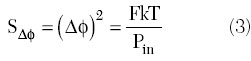
where S??(fm) is determined, using Equation 3, as

taking into account the effect of the signal purity degradation due to the low frequency flicker noise effect close to the carrier, described by the corner frequency fc.

Fig. 2 Equivalent model of a parallel feedback oscillator.
It should be noted that the empirical Leeson equation for S??(fm) contains a multiplication factor of two in the numerator. Moreover, accurate agreement was achieved between the model and experimental results when the power density SDf(fm) was expressed in terms of the compressed (or large-signal) power gain G and output power Pout as S??(fm) = 2GFkT/Pout.4 The parameter F in Equation 6 is associated with the active device noise figure and can be called an effective noise factor because, generally, it should represent the effects of the active device noise sources and the cyclostationary noise resulting from periodically varying processes in practical oscillators. Due to the inherent nonlinear nature of the active device, the effects of intermodulation between the wideband white noise and various harmonics of the fundamental frequency (for example, nonlinear transformation of the noise near the third harmonic downconverted to the near carrier region due to mixing effect with the second harmonic) must be included.2 Also, the effect of low frequency noise modulation of the current, resulting in the reactance modulation of the input impedance of the circuit (for example, variation of the phase angle of the device forward transfer function versus emitter current), cannot be neglected.5 Hence, it is impossible to calculate F accurately without taking into account the effect of the oscillator resonant circuit. Therefore, for such a linear model, the effective noise factor F as well as the corner frequency fc can be considered more like fitting parameters, based on measured data.
The corresponding combined expression to calculate the normalized double-sideband phase noise power spectral density or the double-sideband noise-to-carrier ratio at the input of the feedback oscillator can be obtained from

which gives an asymptotic model showing generally a noise reduction of 9 dB/octave in the offset region with predominant low frequency 1/f noise, 6 dB/octave in the offset region due to feedback loop and 0 dB/octave representing the thermal or white noise spectrum.
The single sideband noise-to-carrier ratio at the input of the feedback oscillator can be described by

whose idealized sideband spectral behavior for different values of the loaded quality factors is illustrated in Figure 3. For the low QL case, there are regions with 1/f3m and 1/f2m dependencies for spectral power density close to carrier, as shown in (a). For the moderate QL case, (b), only a 1/f3m dependence exists as far as the intersection with the thermal noise floor. For the high QL case, (c), regions with 1/f3m and 1/fm dependencies are observed near the carrier. Closest to the carrier, the 1/f3m phase noise behavior is a result of random frequency modulation of the oscillator by low frequency 1/f noise. In the region of 1/f2m phase noise behavior, the white noise causes random frequency modulation. The 1/fm dependence is due to the mixing up of the 1/f noise with the oscillation frequency. Finally, the phase noise becomes constant, which is a result of the mixing up of white noise around the oscillation frequency.

Fig. 3 Single sideband oscillator phase noise behavior.
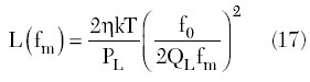
To calculate the same phase noise spectral density at the oscillator output, it is necessary to replace the input power Pin by the power available at the output Pout and to multiply the numerator of Equation 8 by the power gain G. As a result, neglecting the effect of flicker noise and considering the case of fm << f0, one can obtain

is considered the transducer power gain and Q0 is the unloaded quality factor.6 From Equations 8 and 9, it follows that, to minimize the oscillator phase noise, it is necessary to reduce the noise figure F and to increase the input power Pin (or the output power Pout for a fixed power gain G of the amplifier) as much as possible. In addition, for frequency offsets inside the resonator bandwidth, it is desirable to maximize the oscillator loaded quality factor QL. However, the resonator insertion loss and loaded QL are interrelated, and one cannot arbitrarily increase QL without increasing the insertion loss, otherwise a larger power gain G is needed. The two competing effects result in an optimum loaded QL of approximately one half the unloaded Q0 and insertion loss of approximately 6 dB.7,8 Thus, the minimum noise occurs when QL/Q0 = 0.5 resulting in

Note that the difference in the optimum noise performance predicted by different definitions of the output power (power dissipated in the resonant circuit or power available at the amplifier output) is small.6
Now let us represent a parallel feedback oscillator model using the circuit schematic, with an active device and a parallel resonant circuit, shown in Figure 4. Here, the active device is an ideal voltage-controlled current source with transconductance gm. At the operating frequencies of f << fT, where fT is the transition frequency, such a simplified transistor model can describe the behavior of a FET device with the input gate-source capacitance Cgs (it can be included into the resonant circuit capacitance C), the gate-drain capacitance Cgd (its value is typically sufficiently small) and the drain-source resistance Rds (its value is assumed to be infinite). The impedance of the parallel resonant circuit for ?? << ?0, where D? is the offset from the carrier, can be calculated from

where ?0 = 1/?LC is the resonant frequency and QL = ?CR is the loaded quality factor.
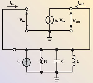
Fig. 4 Equivalent model of a feedback oscillator.
For a given open-loop voltage transfer function H(j?) = gmZL(j?), the closed-loop voltage transfer function T(j?) can be written as
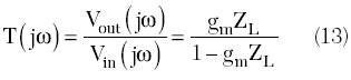
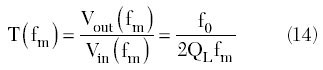
By substituting Equation 12 into Equation 13 and using the steady-state oscillation condition corresponding to the Barkhausen criterion as gmRL = 1, the magnitude T(fm) of the complex transfer function T(j?) can be obtained from
where
![]()
Since the noise current in is produced by the resistor R only, it can be transformed to the equivalent voltage noise with amplitude Vin = ?8kTR?f at the device input. In this case, Equation 14 can be rewritten as

As a result, the single sideband spectral noise power density in a frequency bandwidth Df = 1 Hz, normalized to the total power dissipated in the oscillator P = V2out/2R, can be calculated from

where the factor 1½ arises from neglecting the contribution of the amplitude noise since, for a totally uncorrelated noise, one half of the total noise power contributes to AM sidebands and the other half of the total noise power is converted into PM sidebands.9 Equation 16 is similar to Equation 11 with only the difference in power definitions. Since P represents the total or DC power dissipated in the oscillator with an ideal lossless active device (for example, when the device operates in the switching class E mode), the power delivered to the load is PL = ?p, where ? is the efficiency of the oscillator. The load resistance can represent a part of the resonant circuit resistance R. Thus, Equation 16 can be given in the form
Linear Model for Negative Resistance Oscillator
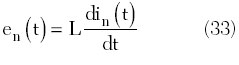
Now consider the equivalent circuit of a simple single-resonant negative resistance oscillator shown in Figure 5, where the available noise power is assumed to be totally from the active device. Here, Rn is the noise resistance associated with active device noise sources, the negative resistance Rout and the equivalent output capacitance Cout represent the device negative output impedance, L is the tank inductance and RL is the load resistance. The derivation of the power spectral density will be based on the fact that the available noise power in the active device is amplified in a frequency selective way, resulting at resonance in the output power PL being dissipated in the load resistance RL.10 This will happen in a steady-state condition when the values of the negative resistance and the load resistance are close to each other.

Fig. 5 Simplified negative resistance oscillator noise model.
Then, assuming that RL + ?R = –Rout and defining the magnitude of the mean-square noise current flowing into the load from the mean-square noise voltage, one obtains

Equation 18 can be rewritten in a common form as

where
?0 = resonant frequency
QL = oscillator loaded quality factor at the resonant frequency
By normalizing the power PL dissipated in the load resistor RL, Equation 18 can be rewritten through the spectral power densities by

where S??= 4kTRn/RLPL and S?= i2nRL/PL is the normalized power spectral density of the noise current across the load resistor RL and ?? = 1 Hz.
Since at small offset frequencies ?m = ? – ?0, close to the resonant frequency,

Equation 20 can then be rewritten in terms of the current and voltage power spectral densities as

which is similar to the power spectral density at frequency offsets close to the resonant frequency for the parallel feedback oscillator. Equation 21 represents a Lorentz function corresponding to an exponential decay of the autocorrelation function in the time domain.11 Since the total output power delivered to the load is equal to PL,
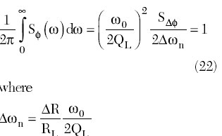
is the Lorentzian linewidth (half-width at half-maximum), which is an oscillator spectrum linewidth characterized by the natural phase fluctuations, due to the thermal and shot noises of the oscillator. However, in a common case, due to the variation of the oscillator resonant circuit parameters, flicker noise, pushing or pulling effects, the effective spectrum linewidth widens, especially close to the resonant frequency.
By using a widely used definition of the loaded quality factor of the passive resonator in the form of

where Dw3dB is the full linewidth at half-maximum, one can write

The normalized power spectral density can be expressed through the Lorentzian linewidth as
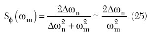
showing a simple linear relationship between the Lorentzian linewidth and the oscillator phase noise spectrum at offset frequencies ?m >> ??n.20 Substituting Equation 24 into Equation 25, and taking into account that F = Rn/RL, results in the single-sideband noise to carrier ratio

which is similar to the Edson noise formula.10,12
Nonlinear Kurokawa Model for Negative Resistance Oscillator
The one-port negative resistance oscillator can generally be represented by the circuit shown in Figure 6. A similar representation of an oscillator circuit can be obtained in terms of admittances. According to the Kurokawa model derivation, based on a small perturbation method, it is assumed that the active device output impedance Zout(A), with a negative real part, is a function of the oscillation amplitude and that the load impedance ZL(?) is a frequency dependent function.22 By considering the sinusoidal current flowing through the active device with a slowly varying amplitude A(t) and phase ?(t) and assuming that the equivalent device noise voltage power can be given by em2 = 4FkTRL?f, the single sideband noise to carrier ratio can be written as

is a function of the oscillator stability conditions, given in parentheses, characterizing the velocity of the establishment of the steady-state oscillators under small perturbations,
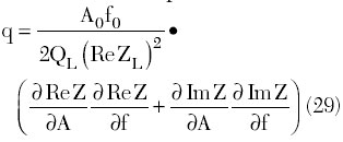
is the parameter illustrating the dependence of the oscillation frequency on the oscillation amplitude in a large-signal mode of operation.

Fig. 6 Equivalent model of a one-port negative resistance oscillator.

is the oscillator loaded quality factor, PL is the output power delivered to the load RL, Z = Zout + ZL is the overall circuit impedance.14
From Equation 27, it follows that the oscillation becomes very noisy as one approaches the boundary of the stable region, that is, as the parameter p becomes close to zero. In addition, the greater the value of the parameter q, the higher the phase noise level is expected in the oscllator spectrum due to amplitude-to-phase conversion. It should be noted that p = 1 when the oscillator circuit is adjusted to maximum power.13
For a particular case of a voltage-controlled oscillator (VCO), when it is assumed that ?ReZ/?f = 0, Equation 27 can be rewritten as

where Re is the equivalent noise resistance of the varactor, KVCO is the oscillator voltage gain in Hz/V.15
Effect of Device and Circuit Nonlinearities
From the Kurokawa model for a negative resistance oscillator, it follows that the nonlinearity of the elements of the device equivalent circuit has a significant impact on the oscillator noise spectrum. The noise analysis, based on the nonlinear MESFET model with dominant nonlinear elements, shows that the gate-source capacitance is responsible for the conversion of low frequency noise into phase noise, whereas the amplitude noise is primarily determined by the nonlinear transconductance.8,16 Compared to the transconductance and gate-source capacitance, the nonlinear drain-source conductance is of minor importance for the noise upconversion process.
As an example, consider an oscillator with a nonlinear output resistance dependent on the applied DC bias voltage and on the amplitude of the self-sustained oscillations. The basic oscillator circuit with the nonlinear negative output resistance Rout, capacitance C, inductance L, load resistance RL and noise current in(t) is shown in Figure 7. The electrical behavior of such an oscillator, in terms of the voltage v(t) across the capacitance, can be represented by a second-order nonlinear differential equation

where
is the equivalent noise voltage and

represents a power series expansion where I0 is the DC current and Gk are the small coefficients.
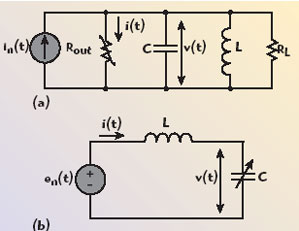
Fig. 7 Second-order nonlinear oscillation systems.
In a steady-state operation mode, when the active device compensates for the losses in the load resistance, that is Rout + RL = 0, Equation 32 can be rewritten as

Seeking the general solution of the inhomogeneous differential equation as the superposition of the general solution of the homogeneous (noise-free) and specific solutions of Equation 35 as
and applying a van der Pol approach for the slowly time-varying amplitude V(t) and phase ?(t), allows rewriting Equation 35 in the form

where ?0 = 1/?LC, and it is assumed that en(t) is a small, slowly time-varying, low frequency noise voltage, for which

As a result, substituting Equation 36 into the right-hand side of Equation 37 and using trigonometric identities yields

which means that the nonlinear output resistance has no impact on the phase fluctuations. However, the amplitude fluctuations are not equal to zero because all factors on the right-hand side of Equation 37 have first-order sine components. Thus, the resistive type of nonlinearities alone would cause amplitude noise only, since the reactive elements determining the oscillation frequency remain constant.
Now consider a varactor-controlled oscillator with the varactor as a nonlinear element whose capacitance depends not only on the applied DC bias voltage but also on the amplitude of the self-sustained oscillations. The basic VCO circuit consists of the varactor with a nonlinear capacitance C, an inductance L and a noise voltage en(t), as shown in the figure.26 The voltage en(t), can represent all the noise coming from both inside and outside the circuit, including any thermal noise from the resistors, flicker noise from the active device and noise from the power supply. The electrical behavior of the oscillator can be described by

where the nonlinear term vdC/dv is included in Equation 40.
By expanding a nonlinear capacitance C into a power series

with small coefficients Ck, substituting Equation 40 into Equation 39 and applying an asymptotic perturbation procedure with decomposition of the perturbed and unperturbed equations, the first-order differential equation for phase fluctuations with the slowly time-varying noise voltage en can be derived as
where V is the voltage amplitude across the varactor.17 Note that the nonlinear capacitance has no impact on the amplitude noise of the oscillator.
From Equation 42, it follows that:
- The first-order capacitance nonlinearity described by the coefficient C1 contributes to the upconversion of the low frequency noise en(t) to the sideband noise near the carrier w0.
- The second-order nonlinearity described by the coefficient C2 generates a phase noise, due to both amplitude-to-phase conversion and low frequency noise upconversion.
- The higher order nonlinearities described by coefficients Ck, k = 3, 4, 5, ..., cause a more complicated noise behavior of the oscillator based on hybrid upconversion and amplitude-to-phase conversion due to cross terms of V and en.
In the case of a single-frequency LC oscillator, the main contributor to the phase noise is the nonlinear collector capacitance of the bipolar device or the gate-source capacitance of the FET device.
In a general case, the equivalent circuit of the active device is very complicated, including both nonlinear intrinsic and linear parasitic external elements. This means that it is difficult to evaluate analytically the impact of each nonlinear element on the upconversion mechanism. Moreover, the joint effect of different nonlinear circuit elements will result in both amplitude and phase fluctuations. Figure 8 shows the nonlinear MESFET equivalent circuit with input and output current noise sources. As can be determined from numerical calculations, the phase noise can be significantly reduced by linearizing both the transconductance gm and the gate-source capacitance Cgs; in other words, both nonlinearities are important contributors to the phase noise.18 The amplitude noise also depends on the capacitance and transconductance nonlinearities. However, the capacitance nonlinearity will not affect the output current if the series gate resistance Rg is set to zero. The nonlinearities of the gate-drain capacitance Cgd and drain-source resistance Rds have negligible effect on the amplitude and phase noise.

Fig. 8 Equivalent circuit of a MESFET device including noise sources.
Conclusion
Both linear and nonlinear phase noise models for the parallel feedback and negative resistance oscillators are discussed in detail, with demonstrations of their advantages and drawbacks. The linear Leeson model for a parallel feedback oscillator is very simply expressed in an explicit analytical form, which can explain the dependence of the oscillator phase noise on the resonant circuit loaded quality factor, signal power, active device noise figure and its low frequency flicker noise. However, it cannot explain the effect of an amplitude-to-phase conversion and higher order harmonics. At the same time, the nonlinear Kurokawa model developed for a negative resistance oscillator demonstrates the explicit analytical relationship between the phase noise and oscillator stability margin, and shows the dependence of the oscillation frequency on the oscillation amplitude in a large-signal operation mode in the form of derivatives of the device and circuit impedances. Also, the individual and joint effects of different nonlinear circuit elements, which will result in both amplitude and phase fluctuations, are analyzed and discussed.
References
1. A. Grebennikov, “Transistor for Wireless Applications: Theory and Design Aspects, Part I,” Microwave Journal, Vol. 48, No. 10, October 2005, pp. 62–78.
2. D.B. Leeson, “A Simple Model of Feedback Oscillator Noise Spectrum,” Proceedings of the IEEE, Vol. 54, February 1966, pp. 329–330.
3. D. Scherer, “Today’s Lesson – Learn about Low Noise Design,” Microwaves, Vol. 18, April 1979, pp. 116–122.
4. T.E. Parker, “Characteristics and Sources of Phase Noise in Stable Oscillators,” Proceedings of the 41st Annual Frequency Control Symposium, 1987, pp. 99–110.
5. D.J. Healy III, “Flicker of Frequency and Phase and White Frequency and Phase Fluctuations in Frequency Sources,” Proceedings of the 26th Annual Frequency Control Symposium, 1972, pp. 43–49.
6. J.K.A. Everard, “A Review of Low Noise Oscillators: Theory and Design,” Proceedings of the IEEE International Frequency Control Symposium, 1997, pp. 909–918.
7. T.E. Parker, “Current Developments in SAW Oscillator Stability,” Proceedings of the 31st Annual Frequency Control Symposium, 1977, pp. 359–364.
8. H.J. Siweris and B. Schiek, “Analysis of Noise Upconversion in Microwave FET Oscillators,” IEEE Transactions on Microwave Theory and Techniques, Vol. 33, No. 3, March 1985, pp. 223–242.
9. C. Samori, A.L. Lacaita, F. Villa and F. Zappa, “Spectrum Folding and Phase Noise in LC Tuned Oscillators,” IEEE Transactions on Circuits and Systems II: Analog and Digital Signal Processing, Vol. II-45, July 1998, pp. 781–790.
10. S. Hamilton, “FM and AM Noise in Microwave Oscillators,” Microwave Journal, Vol. 21, No. 6, June 1978, pp. 105–109.
11. F. Herzel, “An Analytical Model for the Power Spectral Density of a Voltage-controlled Oscillator and Its Analogy to the Laser Linewidth Theory,” IEEE Transactions on Circuits and Systems I: Fundamental Theory and Applications, Vol. I-45, September 1998, pp. 904–908.
12. W.A. Edson, “Noise in Oscillators,” Proceedings of the IRE, Vol. 48, August 1960, pp. 1454–1466.
13. K. Kurokawa, “Some Basic Characteristics of Broadband Negative Resistance Oscillator Circuits,” Bell System Technical Journal, Vol. 48, July-August 1969, pp. 1937–1955.
14. B.T. Debney and J.S. Joshi, “A Theory of Noise in GaAs FET Microwave Oscillators and Its Experimental Verification,” IEEE Transactions on Electron Devices, Vol. 30, July 1983, pp. 769–775.
15. U.L. Rohde and F. Hagemeyer, “Feedback Technique Improves Oscillator Phase Noise,” Microwaves & RF, Vol. 37, November 1998, pp. 61–70.
16. K. Hosoya, S. Tanaka and K. Honjo, “Theoretical Analysis of Relationships Between Resonator Coupling Coefficient and Phase Noise in Microwave Negative-resistance Oscillators,” IEICE Transactions on Electronics, Vol. E87-C, December 2004,
pp. 2132–2142.
17. T. Ohira, “Higher Order Analysis on Phase Noise Generation in Varactor-tuned Oscillators (Baseband Noise Upconversion in GaAs MESFET Oscillators),” IEICE Transactions on Electronics, Vol. E76-C, December 1993, pp. 1851–1854.
18. S. Lee and K.J. Webb, “The Influence of Transistor Nonlinearities on Noise Properties,” IEEE Transactions on Microwave Theory and Techniques, Vol. 53, No. 4, April 2005, pp. 1314–1321.