
A new series of L-band (1200 to 1400 MHz) and S-band (2700 to 3100 MHz and 3100 to 3400 MHz) power solution modules (PSM) has been introduced by Microsemi PPG for pulsed radar applications. These PSMs offer two to three times more output power over the single transistors currently available on the market and are designed with an extremely user-friendly plug-and-play concept such that users can directly drop in and use without further impedance design work. The higher output power and higher efficiency along with the plug-and-play feature can drastically simplify system complexity, rapidly reduce design cycle time, significantly shrinking power amplifier size over 50 percent, and greatly improve production turn-on yield.
Need for Multi-kilowatt Systems with 1 kW or 2 kW as Building Blocks
Discrete high power class-C operated Si bipolar transistors have been widely utilized for L-band (1200 to 1400 MHz) and S-band (2700 to 3100 MHz) pulsed radar applications. Output power levels of these discrete transistors are generally at 200 to 370 W for L-band and 100 W for S-band. However, radar system output power requirements typically are at the multi-kilowatts range, which is far above the power level of a single transistor. Usually a 1 or 2 kW module is designed as the basic building block and then a number of them are combined to achieve the final required system output power.
Challenges with the Traditional Approach
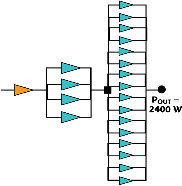
At L-band, one of the most commonly employed configurations for a 2 kW building block module is to employ twenty-one 220 W discrete transistors, such as model 1214-220 M, and use a 1 driving 4 driving 16 configuration, as illustrated in Figure 1. The terminal impedance of this kind of discrete transistor is at the 1 to 2 Ω range; thus, users need to design external input and output matching circuits to transform such low impedance to 50 Ω in order to be compatible with other RF components in the system. Such tasks require specific knowledge, skill sets and experience in the RF/microwave field, and are quite time consuming. Once the individual transistor is matched to a 50 Ω system, the user needs to design both a multi-way power splitter at the input and a multi-way combiner at the output to accomplish driving the inputs and combining the outputs, respectively, of the stage of four and stage of 16 paralleled transistors. The overall module efficiency after such high number of combinations decreases from 50 percent to 35 to 40 percent because of the loss of the 16-way combiner. In addition, the size of such modules tends to be very large; the biasing network and low frequency filtering circuitry for 16 transistors adds another dimension to the overall module complexity. The resulting module is labor intensiveness for production assembly and tuning.
PSM Solution and Benefits
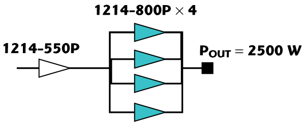
The new PSM Series is designed to provide substantial reductions in system design time, real estate and complexity. Most importantly, users can achieve cost savings in both the design and the manufacturing phases of their system amplifiers while providing considerably higher efficiency, reduced power amplifier size and better system reliability in mission critical applications. Designers can use just one 550, 700, or 800 W PSM to replace up to four 220 W transistors that are commonly designed in parallel at the output of L-band power amplifiers. Figure 2 shows a 2 kW amplifier designed with 1214-800P devices.
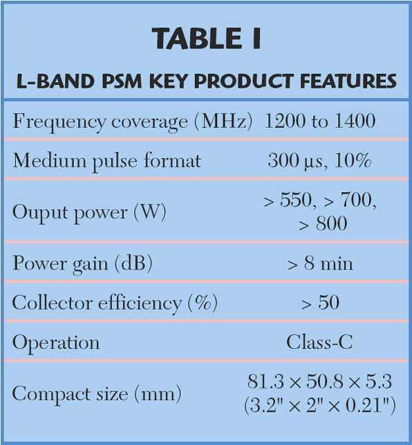
The L-band Power Solution Module Series consists of three model types: the 1214-800P, 1214-700P1 and 1214-550P. They provide a “50 Ω IN-50 Ω OUT” fully matched across the 1200 to 1400 MHz band, high power amplifier stage for pulsed radar systems. These high performance class-C modules are designed for unparalleled performance, delivering peak power outputs greater than 550, 700 and 800 W at 50 percent collector efficiency, under a pulse format of 300 μs, 10 percent long-term duty cycle. Their user-friendly feature provides users with plug-and-play capability that requires no additional tuning or complicated impedance matching.
The PSM product family uses a Microsemi proprietary chip design, effective power combining, and advanced state-of-the-art automated assembly and testing. Its design and manufacturing advantages result in superior performance in power output, gain, efficiency and footprint, while achieving outstanding module consistency and repeatability in high volumes.
Power Solution Module Benefits:
• Extremely easy to use—50 Ω IN-50 Ω OUT— plug and play
• Significantly reduced design cycle—No complex RF impedance matching work required
• Reduced system size—PSM devices are compact
• Reduced system complexity—fewer combining stages required; no matching necessary
• Improved system performance—high efficiency, reliability and repeatability
• Eliminates system production transistor assembly and RF tuning time
• Greatly improves production yield—reduces transistor scrap
• Reduces system components inventory
• Custom-designed PSM to customer’s specifications available
PSM Key Specifications and Design Approach
The NPN silicon bipolar junction transistor used in the PSM is designed and fabricated at Microsemi PPG - RF Products Division. Table 1 lists the L-band PSM’s key features. The transistor has an interdigitated geometry with very tight emitter-to-emitter pitch to increase the emitter periphery-to-base area ratio, which on this chip is about 8 mil. The emitter periphery and epitaxial material was chosen to provide nominal power of 100 W per chip biased at 50 V. Double layer gold metallization is used to lower the output capacitance (COB) and also results in achieving excellent MTTF for the L-band frequency range. Nichrome emitter ballast resistors are used for better linearity.
The transistor chips are attached to a 40 mil thick metallized beryllium oxide (BeO) substrate over a 60 mil thick CuW flange. The packaged transistors are internally matched with input and output metal-nitrate-metal (MNM) capacitors that are also fabricated at Microsemi PPG-R. The input matching network consists of a two-stage low pass impedance matching transformer design by using the series inductance of bond-wires and capacitance of shunt MNM capacitors soldered to the metallized ground plane. Output matching consists of the shunt inductive bond-wires connected from the isolated collector-die attachments area to DC blocking capacitors, which are also mounted on the metallized ground plane.
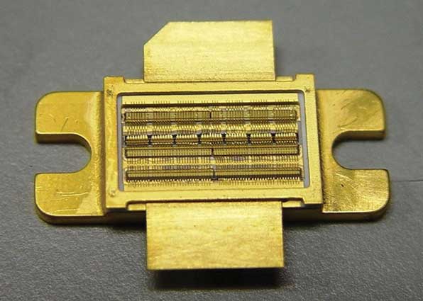
All bond-wires are straight and in-line, which allows fully automatic wire bonding for mass production and consistency. All together there are 369 wire bonds. Figure 3 shows the inside of the single-ended transistor. These transistors are hermetically solder-sealed for the highest reliability.
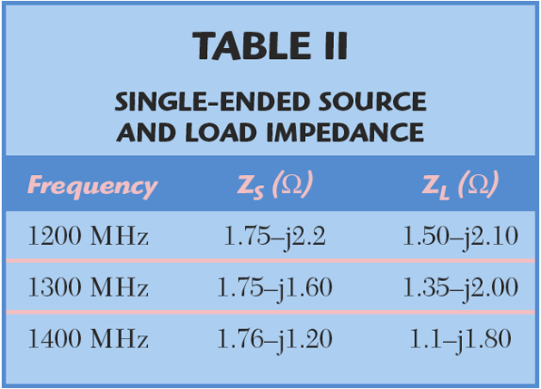
The single-ended input and output impedances achieved with the internal matching design are shown in Table 2. The source impedance ZS and load impedance ZL are measured using a TRL technique and are oriented away from the transistor.
This Power Solution Module is designed on Roger Corp.’s RT/Duroid copper-backed boards. The compact size of the 1214-800P PSM (81.3 mm x 50.8 mm x 5.3 mm) makes it very attractive for users who have constraints on system mechanical dimensions. The surface of the board is also electro-plated to prevent the oxidation of the copper boards.
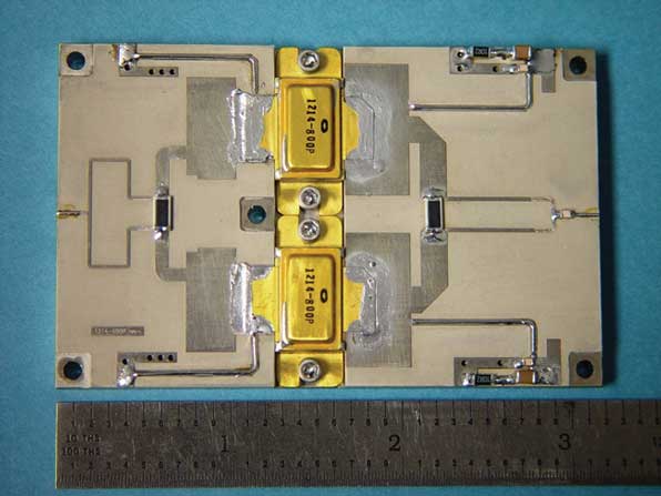
The power combining technique used in this power amplifier is a Wilkinson divider/combiner. Impedances of the input and output of the single-ended transistors are first transformed to a 25 Ω intermediate impedance. This impedance is subsequently transformed to 50 Ω through the Wilkinson divider/combiner. The two RF choke sections are set to be quarter-wave length at 1300 MHz. Two 50 Ω high power AlN resistors, one for each side of the divider/combiner circuit, are used to provide isolation between the two single-end transistors. The isolation is more than 20 dB according to computer simulation. To achieve higher output power and high efficiency the transistors are configured in common base mode and class-C biased. The 800 W Power Solution Module described here is shown in Figure 4.
RF Measurements And Performance
To facilitate the demonstration of PSM performance, a test fixture was built where SMA connectors could be attached to the input and output of the RF terminals. Two high voltage 4000 μF storage capacitors are also soldered to the biasing circuits, one on each side of the PSM. Finally, a heat dissipating aluminum fin is mounted on the bottom of the PSM and an air-cooling fan is used to cool the PSM during test.
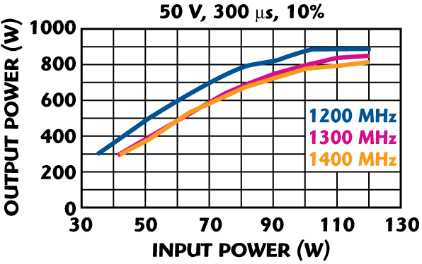
The performance of this 800 W PSM tested under 300 μs pulse width, 10 percent duty cycle biased at 50 V is shown in Figures 5 and 6. The output power is measured at the middle of the pulse, which is 150 μs into the pulse for this case. As shown, 800 W of output power is obtained with input power drive at about 110 W, which corresponds to 8.6 dB power gain at frequency of 1400 MHz. At 1200 MHz, 893 W of output power was measured at the same input drive, which is 9.1 dB gain.
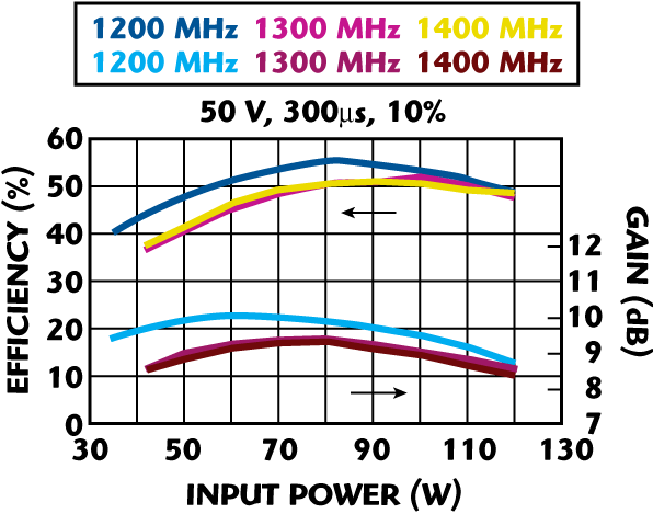
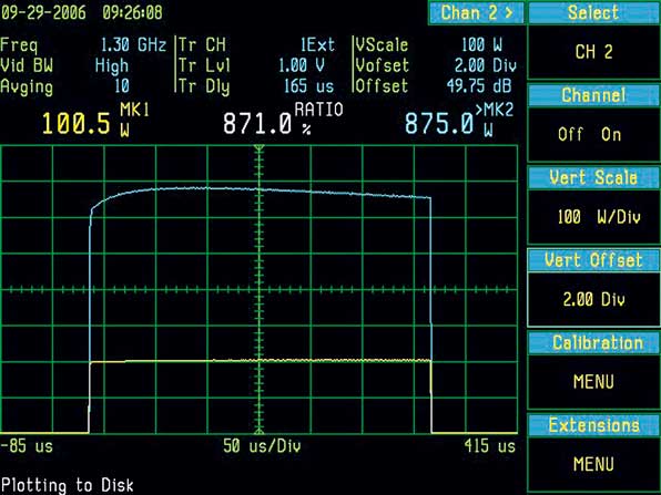
The output gain flatness for this power module is less than 0.5 dB measured at this fixed input drive. The collector efficiency is around 50 percent at Pin = 110 W. A snapshot of a typical pulse shape at 1300 MHz is shown in Figure 7. The typical amplitude droop is under 0.3 dB, an indicator of excellent thermal design. The return loss across the frequency of 1200 to 1400 MHz is better than –12 dB.
PSM Family for S-band Pulsed Radar Applications
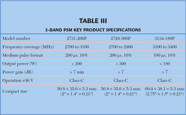
The demand for a similar product for S-band pulsed radar applications has been increasing. The PSM family also consists of three platform products that cover the popular 2700 to 3400 MHz frequency range: 2731-200P, 2729-300P and 3134-180P, as listed in Table 3.
Design Philosophy and Mass Production Capability
Consistency is at the heart of chip development discipline. Thermal die simulation and thermal scan analysis guide die design to eliminate hot spots, produce thermally balance die with targeted low junction temperatures that permit consistent die operation and the utmost reliability. Fully automated die attach, wire bonding and assembly assures precise construction and tight tolerances of all critical elements and dimensions. Automated RF test guarantees repeatable RF performance. As a result, the consistency and repeatability of critical parameters for phase array radar applications, such as output power, gain and insertion phase from lot to lot are able to achieve extremely tight distribution in volume production.
Conclusion
Power solution modules have been described that feature a plug-and-play concept that has built-in impedance transformation networks with 50 Ω terminal impedance at both input and output. Users can easily drop in the PSM to their system power module without any further impedance design work and enjoy the benefits of faster design cycle time, simplified power module complexity, reduction of system size, improvement in system reliability, elimination of production tuning, improvement of transistor yield, and reduction of inventory of components count in addition to the obvious enhancement of higher power and higher efficiency.
Microsemi Corp.
Power Products Group
Santa Clara, CA (408) 986-8031
www.microsemi.com