
IC packaging has become a critical bottleneck to achieving further reductions in the size of wireless products. While Moore’s law provides a continuous increase in the density of digital silicon components with each new process node, there is no Moore’s law for the RF components used in today’s broadband wireless products.
SOC solutions to medium power, multi-band RF products have not proven to be acceptable in most applications and thus RF front ends are still composed of heterogeneous RFIC technologies along with discrete passive components. As a result, RF modules are rapidly becoming the standard form for packaging high frequency microwave components for consumer wireless applications. The rapid growth in wireless-capable products (approaching 2 billion devices annually), growing complexity of wireless technologies (such as MIMO and OFDM), proliferating frequency bands and standards is challenging conventional SMT based designs. These drivers plus continuously shrinking form factors has pushed the RF design task back into the RF semiconductor supply chain and required dramatic reductions in the bill of material through the integration of active and passive components. By tightly integrating RF ICs and high performance passive components, a System-On-Package (SoP) approach to RF design is creating a new generation of RF modules with significant space and cost savings over conventional SMT assembly with discrete components. JMD has developed a new, patented process to implement RF SoP Known as Multi-Layer Organic packaging (MLO), this process provides a vehicle to embed most of the critical RF passive components in a wireless product into a substrate underneath the RFICs while maintaining high performance. MLO represents a major innovation in both process and design. More than just a packaging technology, MLO represents a fundamental change in the method of designing compact RF systems.
I. MLO History and Status
MLO is an outgrowth of packaging research funded by the National Science Foundation at the Georgia Tech Microelectronics Packaging Research Center. Although there are multiple packaging alternatives for 3D System-In-Package (SiP) applications, the research conducted at Georgia Tech has focused on SoP solutions where thin-film materials and embedded components are inherent in the approach as opposed to simple SiP packages that combine die and SMT components into over-molded packages. Over the past few years this technology has applied to develop highly integrated RF front-end-modules (FEMs) for consumer wireless applications [1].
The use of highly integrated FEMs is especially critical for products based on standards such as 802.lln and 802.16e which rely on MIMO systems and OFDM modulation. MIMO and OFDM are important drivers since they require 1) multiple transmit and receive paths (often operating over multiple frequency bands) and thus multiple power amplifiers (PAs) and associated filtering components and 2) highly linear PA and LNA circuits which must provide high gain and low distortion in the presence of interfering signals and spurious signals from digital circuits. These factors in turn have dramatically increased the number of passive components required further challenging packaging technology.
Other alternatives for RF multi-chip packages such as LTCC and silicon or GaAs integrated passive devices have significant limitations addressing the demands for increased complexity and shrinking geometries. SOC approaches to integrate front ends have largely failed to deliver on their promises other than for very simple wireless devices. LTCC is a mature packaging technology but is costly to produce and suffers from temperature related failures due to CTE mismatch with common printed circuit board materials. It is also difficult to integrate RF, digital and mixed-signal technologies in LTCC due to package size limitations.
A number of products have been developed that leverage the rapid turn-around, and high integration capabilities of MLO. Early products were integrated passive devices (IPDs) designed as alternatives to conventional ceramic RF filters and baluns for satellite, cellular and WLAN frequency bands. By using novel, lumped element filter topologies and the very high density and high Q structures provided by MLO, these products replaced multiple ceramic components and yielded significant reductions in PWB real estate along with savings in assembly and test.
Figure 1 shows two examples of MLO IPDs designed for WLAN and satellite TV applications. The diplexer measures 5x20mm and contains the equivalent of 35 capacitors and inductors.

Fig. 1 MLO (a. Satellite Diplexer and b. WLAN balun IPDs)
The WLAN balun is only 2x1.25x.5mm. [2], [3] By reducing the thickness of the stackup, MLO can also be used for RF module substrates. A derivation of the original MLO process was developed that results in very high circuit densities (>400 components per square centimeter) in substrates of only 500-600 microns thick. Comparable or better performance is obtained with only six metal layers of MLO compared to 12-20 layers of LTCC. While there have been other attempts to embed passive components into organic laminates, most of these have addressed non-RF passives such as resistors and decoupling capacitors.
Low value RF inductors are sometimes etched into the copper on the top layer of FR4 RF IC substrates, however FR4 and similar laminates are very lossy above 1 GHz and as a result can not produce the high Q embedded components (inductors and capacitors) required for critical filters and matching circuits. MLO is the only laminate packaging process that can displace essentially all RF passive functions found in the typical wireless front-end.
II. MLO Module Construction
A MLO substrate consists of one or more RF dielectric layers embedded between layers of other laminates to provide routing, shielding and bonding areas for SMT and RFIC die placement. A typical “stackup” is shown in Figure 2.
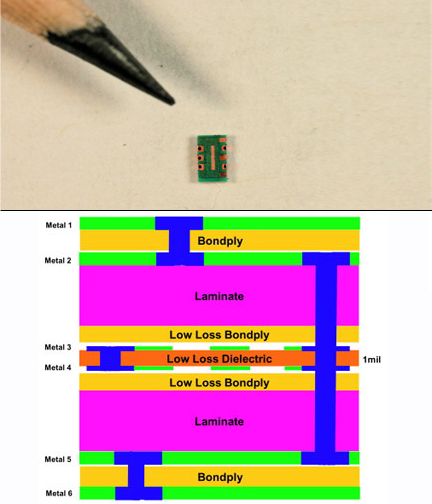
Fig. 2 MLO Stackup
Variations of this stackup may be used if, for example, thinner substrates are required. The dielectric layer must have low loss at the common wireless frequency ranges and at the same time have a high dielectric constant (Er) to provide high capacitance density.
Unfortunately these are counteracting properties for most materials since a high Er is usually obtained by filling polymers with dielectric materials which can increase loss. For this reason very thin dielectric layers are necessary. Recently a number of low-loss formulations of liquid crystalline polymer (LCP) and fluropolymers (PTFE) have become available in copper clad films as thin as 25 microns [4]. LCP is an unfilled material with a low Er that has been shown to have very favorable characteristics for a wide variety of RF and high speed application [4]. In the case of PTFE, advanced filler materials are used to increase Er without significantly increasing loss. By carefully selecting other laminates and bond ply materials it is possible to utilize standard lamination processes to produce high performance RF packages.
Once the module design is completed, the six metal layers of the stackup are etched and assembled. Metal layers 1 and 6 contain the component layouts and LGA pad patterns respectively while metal layers 5 and 2 are primarily for routing and shielding. The most critical step in the MLO process is the exposure and etching of the inductor and capacitor structures into layers 3 and 4 as shown in Figure 3.

Fig. 3 MLO Substrate Layers (M1-M6)
To achieve the desired component densities line widths and spacings on the order of 50 microns are used with the potential for further increases in component density by reducing line widths and spacings to 25 microns. Since these components form the resonant structures of the embedded components, they must be reproducible with high precision. As no manufacturing process will be perfect, it is essential to design RF structures that are also tolerant to process variations. An extensive modeling capability for MLO RF structures has been developed and incorporated this capability into unique tools that provide the designer with a choice of components with known tolerances and yields. The 3D interconnection of substrate layers is another critical element in achieving high circuit density without sacrificing RF performance. Vias add inductance and must be fabricated carefully to minimize their effects and to achieve high fabrication yield. Once a MLO substrate is fabricated, standard SMT and die attach steps are utilized to complete the module. Figure 4 shows a strip of assembled modules ready for encapsulation and simulation.

Fig. 4 Assembled MLO Strip
III. Process Control
An essential requirement for putting MLO based products into volume production is the ability to monitor process parameters and to predict their impact on device yield. Although fabricated from laminate materials, a MLO panel (typically 12 x 18 inches) is treated like a RF semiconductor wafer from the standpoint of process control and testing. The most critical parameters for controlling embedded component tolerances are of course the core layer thickness, layer-layer registration and line width and spacing on the dielectric layers. The derivation of these parameters is a very complex process involving tradeoffs between fabricator capabilities and RF design parameters. Since tighter control over these critical parameters will inevitably lead to higher costs, JMD has developed process tolerant component designs that can produce high yields without requiring significant new investment in fabrication technology. Design for manufacturability (DFM) has been an important element of the development of MLO. JIMD has developed a number of proprietary tools that facilitate the designer’s task of developing high yield products. As in semiconductor fabrication, process control monitor (PCM) structures are utilized with MLO to allow rapid measurement of key process parameters post fabrication. Along with automated optical inspection (AOl) data, PCM measurements are used to refine device models and to provide feedback to laminate fabricators. Novel PCM structures have been developed that yield measurements that are highly correlated with material and process parameters by using simple DC and low-frequency probes.
Figure 5 shows a typical MLO strip layout and associated PCM structures.

Fig. 5 MLO Strip with PCM Structures
Figure 6 shows a cross section of an assembled module and the exposed edges of copper conductors and a via profile.
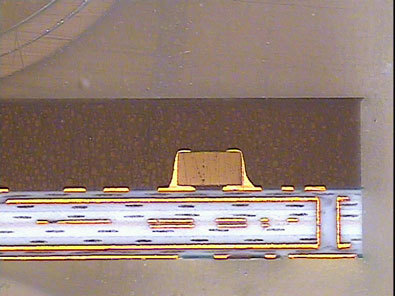
Fig. 6 Module Cross Section
IV. RF Component Structures
To take full advantage of the embedded device capabilities of MLO, product designers need the ability to rapidly implement the common components used in RF systems such as matching networks, filters, baluns, couplers and diplexers. These components can be implemented in a wide range of circuit topologies but must be ultimately transformed into lumped element structures consisting of embedded inductors, capacitors and transmission lines. Because small form-factor packages require very high component densities, these structures must be designed to provide the desired level of performance in the presence of coupling and ground conductor proximity. The Q factor of embedded components is also critical to ensure low-loss. Particularly in inductor design, structures must be modeled and tested to insure that the desired Q factors can be maintained. For this reason the designers must be provided with ‘known good structures’ for common functions at the various frequency bands used in wireless systems. Inductor Qs of over 150 have been achieved at 3 GHz with MLO [1]. This compares with Qs of 20-50 with silicon IPDs or conventional laminates. An example of such a re-usable structure is shown in Figure 7.

Fig. 7 2.6 GHz Bandpass Filter Implemented in MLO
The 2.6 GHz balanced bandpass filter was initially synthesized using standard RF design tools and then implemented in a two-layer spiral structure. The filter achieves an in-band insertion loss of 1.8 dB, and out of band rejection from 4.1 to 4.5 GHz of 40 dB and 45 dB below 2 GHz.
One of the most significant benefits of having complete control over embedded passive components is that it provides the designer with the ability to achieve an almost arbitrary impedance transformation between what is presented by RF ICs and other cascaded circuit elements. For example, most power amplifiers (PAs) and low noise amplifiers (LNAs) used in microwave circuits are designed to present 50 ohm input and output impedances. While it is necessary to have an agreed upon standard impedance (i.e. 50 ohms) when using conventional circuit design topologies involving packaged RF ICs and packaged ceramic passive components (filters, baluns, etc.), it is not required when bare die are used in a module using embedded inductors and capacitors. In spite of the stated data sheet performance parameters for these devices assuming a 50 ohm match, they may not actually exhibit a pure 50 ohm resistive load under all conditions. Thus it is possible and practical to improve the RF IC’s performance by providing some other impedance in the input or output. In addition, the designer of an embedded filter component can “pull” the RF IC’s match and change its load line, thereby achieve additional design flexibility such as optimizing EVM or noise figure over gain. Unlike conventional packaged ceramic components, MLO lumped elements allow any value of inductance or capacitance to be achieved (within the limits of the process) and thus provide many more degrees of freedom when designing wide-band microwave circuits with demanding linearity and efficiency requirements.
In one sense the MLO design process is a continuation of the RF IC design process which seeks to optimize gain, power output, linearity, etc. within the constraints of a particular process and with the highest yield. By considering the die and package as a single component, optimum performance can be achieved by minimizing the use of lossy on-chip passives.
V. Design Flow
Efficient design of RF front-end systems with embedded components requires a unique design flow as well as tools that are not included in commercial RF EDA packages such as Sonnet, ADS, and HFSS. A typical design flow for a MLO product is shown in Figure 8.

Fig. 8 MLO Module Design Flaw
Three primary objectives drive the continuous improvement in design flow and tools, -reduction in design cycle time (DCT), excellent model to hardware correlation and accurately predicting production yields.
Process distribution data is the key data feedback loop between the substrate foundries and DFM support tools. By extracting process data from AOl and PCM measurements, designers are presented with layout alternatives for inductors and capacitors that have known characteristics over large production runs. Of course the ultimate aim of the design flow is to produce complete products. Figure 9 shows a block diagram and final package of a lx1 dual band WILAN front-end module used in IEEE 802.lln applications.

Fig. 9 1x1 Dual Band FEM for 802.11n
This particular example of a MLO module is only 6.6x5.4x1.2mm and contains three active die, over 100 embedded passive components and only 12 SMT components that could not be economically embedded. When used in a typical 802.11 n application it requires no external components other than bypass capacitors on the PWB.
VI. Future Direction for MLO
Now that the basic capabilities of organic packages for complex RF systems have been demonstrated, there are many exciting areas where MLO can be extended for a broader range of applications. Research conducted at Georgia Tech has already shown interesting results in using organic polymers for RF MEMs applications [5] and for multi-frequency signal generators [6]. Antenna integration into organic structures is another active area of research at Georgia Tech [7] and potentially could lead to tighter integration between RF front end components and antennas in the same package. A third area of research involves identification and selection of other laminate systems with higher Er to increase component density. Perhaps the most significant potential for future organic RF packages is the possibility of removing passive components from RFICs and placing them into the substrate. The basic MMIC premise of single packaged die with 50 ohm interfaces is not required in high performance multi-chip organic packages. In fact an argument could be made that significant cost savings could be obtained especially in the case of GaAs RF ICs if die sizes could be reduced as a result of moving passives into the substrate. By using organic packaging technology to the fullest extent, RF engineers will be able to have their own “Moore’s Law” for complex RF circuits.
References
2. V. Govind, P. Monajemi, L. Carastro, S. Lapushin, C. Russel, S. Dalmia, J. Vickers, V. Sundaram and U. White, “Design of novel highly integrated passive devices for Digital Broadcasting Satellite/802. 11 home networking solution in Liquid Crystal Polymer (LCP) based organic substrates”, IEEE MTT-S International Microwave Symposium (IMS) Digest, San Francisco, CA, Jun. 2006.
3. V. Govirid, W. S. Yun, S. Dalmia, V. Sundaram, G. E. White and M. Swaminathan, “Analysis and design of compact wideband baluns on multilayer Liquid Crystalline Polymer (LCP) based substrates”, IEEE MIT-s International Microwave Symposium (IMS) Digest, Long Beach, CA, Jun. 2005.
5. G. Wang, D. Thompson, M. M. Tentzeris and J.Papapolymerou, “Low Cost RF MEMS Switches Using LCP Substrate,” European Microwave Conference, Amsterdam, The Netherlands, October 2004.
6. S. Dalmia, A. Bavisi, S. Mukerjhee, V. Govind, V. Sundaram, G. White, and M. Swaminathan, “Multiple Frequency Signal Generator for 802.11 a,b,g VU WLAN type Applications Using Organic Packaging Technology”, Proceedings from the IEEE ECTC 2004.
7. N. Altunyurt, M. Swaminathan, V. Sundaram and G. White, “Conformal Antennas on Liquid Crystalline Polymer Substrates for Consumer Applications”, submitted to Asia-Pacific Microwave Conference, 2007
JMD • 75 5th Street • Atlanta, Georgia 30308 • (404) 961-7240 • www.jacketmicro.com