In the design of high frequency power amplifiers, one of the parameters is the stability of the active device. The stability of the active device is determined by the Rollet stability factor K.
If K > 1, then the active device is unconditionally stable and the design of the amplifier is based on conjugate matching to obtain the maximum power gain.
If, however, K < 1, the device is potentially unstable and the design is based on a trade-off between the gain and stability of the amplifier.
In the realization of a practical amplifier, it is usual to ground the active device using vias.
Consequently, the manufacturer’s S-parameters are modified by the positive feedback produced by the lead and via inductances that could make the amplifier potentially unstable.
A further problem in the realization of a practical amplifier is the design of the bias circuit used to ensure that the active device is operating at the manufacturer specified DC condition.
The bias network should be designed so that it has a minimum effect on the gain of the amplifier and produces minimum feedback over a wide frequency range. The latter point is particularly important in the design of multi-stage amplifiers.
In this article, it is shown that if the vias are placed as close as possible to the edge of the chip and by using a number of vias, the stability of the amplifier is improved.
Also, if the bias network designed has less RF signal leakage over a wide range of frequencies, flatter gain of the multi-stage amplifier can be achieved.
Based on the above investigations, single-ended, balanced and two-stage amplifiers operating at 2.45 GHz have been designed, and the measured results obtained are in good agreement with those predicted by simulation.
Effect of Via and Lead Inductances on the Stability of the Amplifier
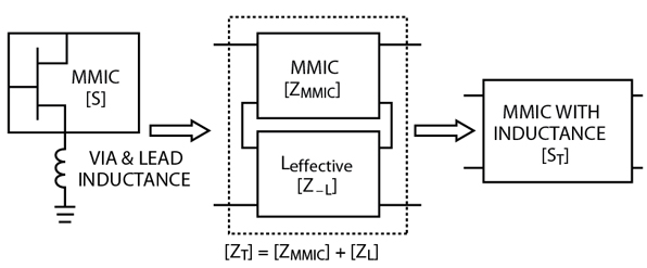
An active device has input and output leads, and two additional leads that must be grounded, as shown in Figure 1. Due to the physical constraints it is not possible to ground these two terminals at the edge of the chip using vias.
The vias must be connected a small distance from the edge of the chip, hence introducing lead inductance. The via itself also behaves as an inductor. These parasitic inductances cannot be neglected at high frequencies.
The overall S-parameters of the grounded MMIC include the effective lead and via inductances. By treating the active device and the via/lead inductances as two, two-port networks connected in series, the overall S-parameters can be obtained, as shown in Figure 2.

The Rollet stability factor K1 can be obtained using the manufacturer’s S-parameters. However, the overall S-parameters should be used in Equation 1 for the grounded MMIC.
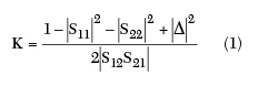
For the active device to be unconditionally stable, K must be greater than 1 and |Δ| < 1
where
Δ = S11 S22–S12 S21
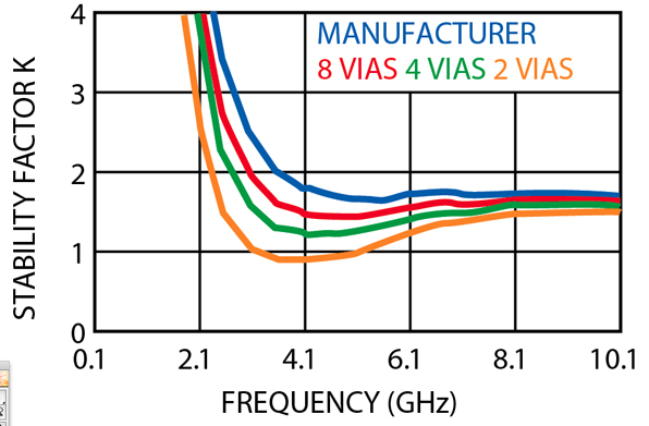
Using Microwave Office 2001 and neglecting the effect of the lead inductances, Figure 3 compares the stability factor K based on the manufacturer’s S-parameters with that of the grounded MMIC chip (MGA 86576 from Agilent) using a number of vias. The substrate used was FR4 PCB having a thickness of 0.79 mm and relative permittivity, εr = 4.3.
As can be seen, the MMIC based on the manufacturer’s S-parameters is unconditionally stable, but for the practical case using two vias it becomes potentially unstable.
The grounded MMIC can be marginally unconditionally stable using four vias; the stability can be further improved by using eight.
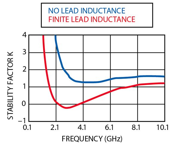
Figure 4 shows the effect of only the lead inductance on the stability factor K for four vias placed 0.5 mm away from the MMIC chip. Figure 5 shows the effect of the vias and that of the lead inductance on the stability factor K.
It can be seen that the effect of the via inductance is negligible on the stability factor for the substrate having a thickness of 0.79 mm. If a thicker substrate was used, then the via inductance would have a more significant effect and should be taken into account.
Effect of the Bias Network on the Gain of the Amplifier
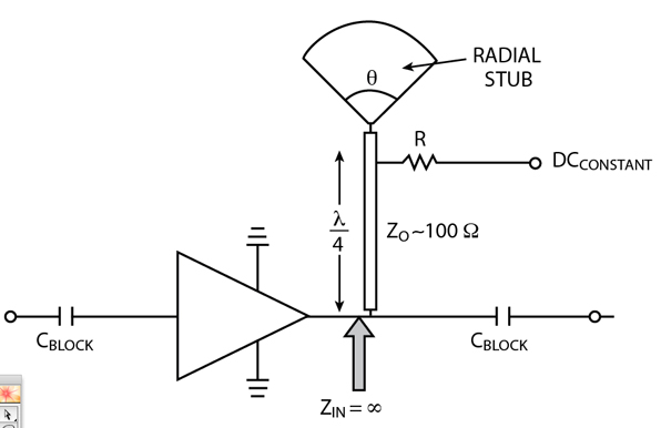
The bias circuit is designed to reduce leakage of the signal and hence have a negligible effect on the gain of the amplifier. For a multi-stage amplifier design, it is even more important to reduce the leakage, as this reduces the feedback making the amplifier more stable. Figure 6 shows a typical bias circuit using a radial stub as an effective capacitor.
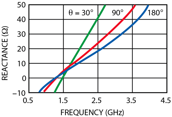
The reactance of the radial stub for θ = 30°, 90° and 180° is shown in Figure 7. By using a half-moon radial stub (θ = 180°), a broader band RF open circuit can be achieved for this bias circuit.2
Note that, for all the lumped components, equivalent circuits were used in the simulations.
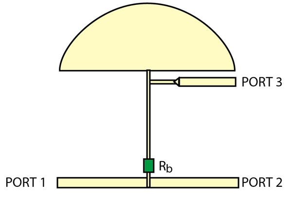
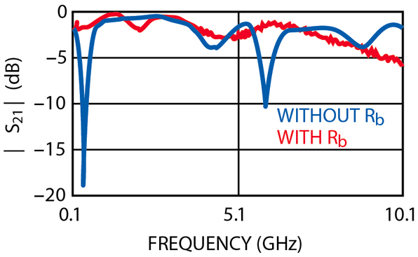
The frequency response for the fabricated bias circuit (see Figure 8) is shown in Figure 9. By placing the bias resistor Rb close to the feed line, the forward transmission coefficient |S21| has a broadband response and the RF leakage signal is minimized over a wider range of frequencies.
The leakage signal can be further reduced by using a number of chip capacitors and quarter-wave transformers, as shown in Figure 10.
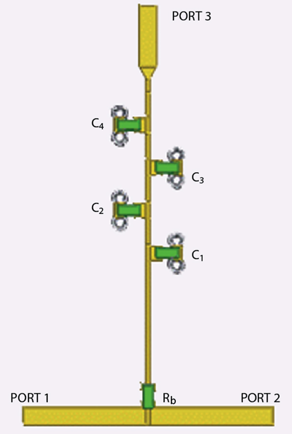
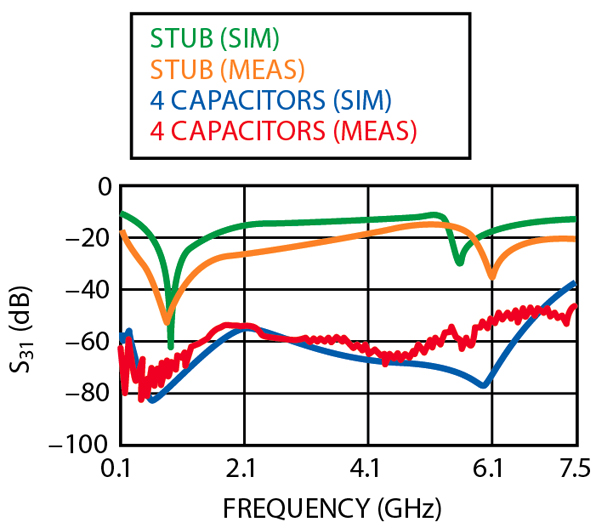
Figure 11 shows the measured and simulated responses of the two bias networks showing excellent reduction of the leakage signal over a wide range of frequencies for the new design. This form of bias network should be used in the design of broadband and cascade amplifiers.
Design of a Single-ended and Balanced Amplifier
The maximum power gain of an amplifier can be obtained by conjugate impedance matching using the source and load reflection coefficients1
where
B1 = 1 + (|S11|)2 | (4a) | |
– (|S22|)2 – (|Δ|)2 | ||
B2 = 1 – (|S11|)2 | ||
+ (|S22|)2 – (|Δ|)2 | (4b) | |
C1 = S11 – ΔS22* | (5a) | |
C2 = S22 – ΔS11* | (5b) | |
Δ = S11S22 – S12S21 | ||
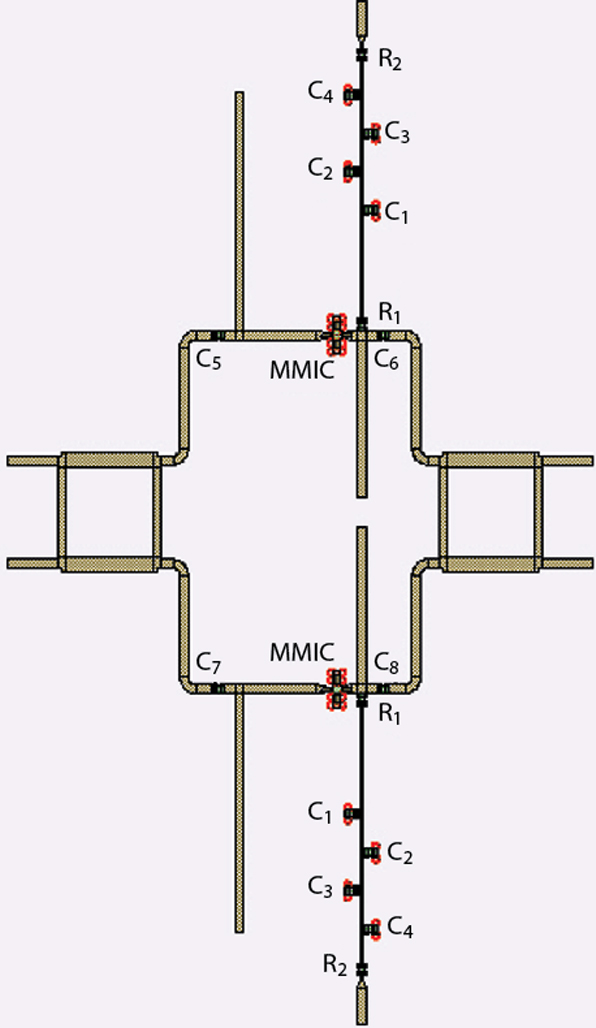
At 2.45 GHz, for MGA 86576, ΓSM = 0.45 –81.4° and ΓLM = 0.31 –76.7°. The input and output matching networks were designed using a Smith chart before simulation. Two blocking capacitors are placed at the input and output of the circuit. The bias circuit used is the improved one shown previously. The balanced amplifier was then designed by incorporating single-ended amplifiers between a pair of 3 dB directional couplers, as shown in Figure 12.
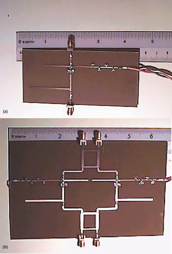
The single-ended and balanced amplifier circuits were optimized to obtain maximum gain and to be stable over the frequency range of 2 to 2.7 GHz. The layouts of the practical amplifiers, single-ended and balanced, are shown in Figure 13.
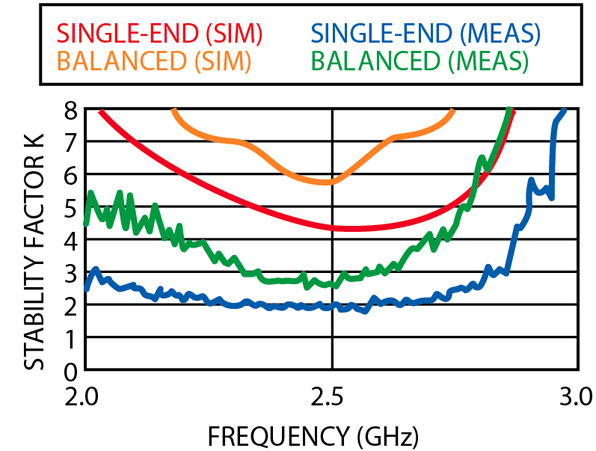
Figure 14 shows the simulated and measured stability factor for the single-ended and balanced amplifiers demonstrating that they are unconditionally stable over the specified operating frequency range.
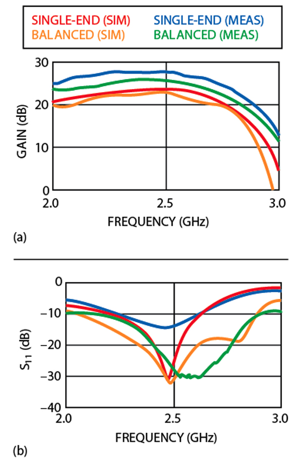
The simulated and measured gain and return loss for both amplifiers is shown in Figure 15.
There is good agreement between simulation and measurements. The impedance matching and stability of the balanced amplifier is improved, compared to the single-ended configuration.
Performance of a Two-stage Cascade Amplifier
The design presented in this section is meant to show that the new bias circuit produces a stable broadband two-stage amplifier. In this design, the single-ended amplifier is miniaturized by first normalizing Zo to 83 Ω (W = 0.51 mm for a substrate with εr = 4.3 and H = 0.79 mm) to match the dimension of the input and output leads of the MMIC to the width of the microstrip line.
Based on the Bode-Fano criterion,3,4,5 a theoretical limit of the minimum reflection coefficient can be achieved with an arbitrary network. Here, the existing matching network was optimized by selective mismatching to compensate for the variation of the gain versus frequency of the MMIC to produce a broadband gain response.
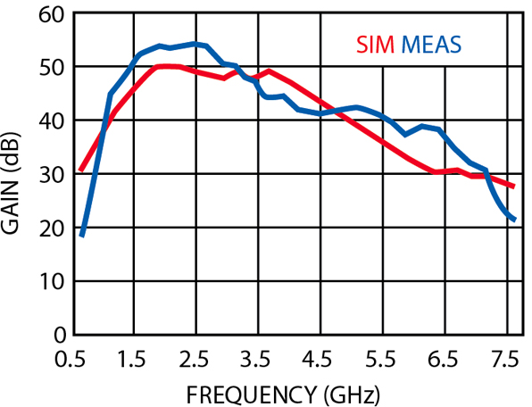
The layout of the two-stage amplifier is shown in Figure 16, while the realized circuit is shown in Figure 17. The gain versus frequency response of the amplifier is shown in Figure 18 and, as can be seen, a gain of over 30 dB has been achieved from 0.8 to 7.0 GHz.
Conclusion
The S-parameters given by the manufacturer show that the MMIC MGA 86576 is unconditionally stable.
However, when grounded, the MMIC can become potentially unstable due to lead and ground inductances.
The stability of the amplifier is improved considerably by using a thin substrate, placing the vias as close as possible to the chip and increasing the number of vias used.
The input signal leakage can be reduced considerably by using the proposed bias network, consisting of a number of chip capacitors and a number of quarter-wave transformers.
This bias network can therefore be used to produce a stable multi-stage amplifier.
References
1. D.M. Pozar, Microwave Engineering, Second Edition, John Wiley & Sons Inc., New York, NY 1998.
2. B.A. Syrett, “A Broadband Element for Microstrip Bias or Tuning Circuits,” IEEE Transactions on Microwave Theory and Techniques, Vol. 28, No. 8, August 1980, pp. 488–491.
3. H.W. Bode, Network Analysis and Feedback Amplifier Design, Van Nostrand, New York, NY 1945.

4. R.M. Fano, “Theoretical Limitations on the Broadband Matching of Arbitrary Impedance,” Journal of the Franklin Institute, Vol. 249, pp. 57–83.
5. V. Kaman, “A 100 kHz to 50 GHz Traveling-wave Amplifier IC Module,” IEEE Microwave and Guided Wave Letters, Vol. 9, No. 10, October 1999.