

Grayzel1 presented the theory of the Grayzel narrowband negative resistance amplifier (GNRA)2,3 with experimental confirmation. The gain as a function of frequency of a negative resistance amplifier that used an operational amplifier to generate the negative resistance and a circulator at its output was measured. The amplifier can operate at any frequency where there is negative resistance and is not dependent upon how it is realized.
This article describes the design of a negative resistance amplifier using a 3 dB directional coupler or hybrid coupler and matched tunnel diodes. Diodes produced from the same wafer are very closely matched, and the value of the negative resistance can be fine-tuned by “tweaking” the bias voltage. MMIC miniature 3 dB directional couplers have been developed,4-6 and their small footprints make the GNRA suitable for cell phones and other hand-held communication or military devices.
Superconductor filters are currently used in various applications, particularly in communication systems and scientific research, where very narrowband filters are required.
Mobile communication base stations use them to enhance signal quality, and radio astronomers use them to improve the sensitivity of radio telescopes. Additionally, military communication systems, radar and other areas requiring narrowband filters employ superconductor filters. The GNRA, once fully developed, will be able to replace them.
A 2.9 GHz tunnel diode amplifier is analyzed, and its gain is simulated as a function of frequency. Tunnel diodes are very low noise devices and can operate at very high frequencies.7 It is shown that negative resistance amplifiers with bandwidths of less than 0.004 percent are achievable.*
*Patents US11,863,131 B1 and US12,052,002 B2
25 DB NEGATIVE RESISTANCE AMPLIFIER DESIGN
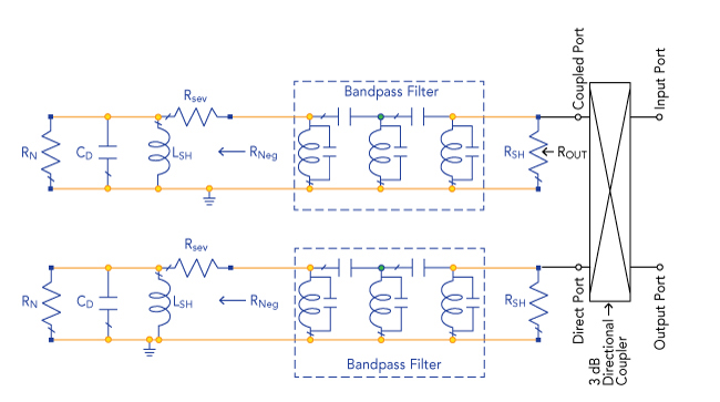
Figure 1 Tunnel diode negative resistance amplifier schematic.
Figure 1 shows the schematic of a tunnel diode negative resistance amplifier. Two identical negative resistance circuits are connected to a 3 dB directional coupler; one is connected to the direct port and the other is connected to the coupled port. An ideal directional coupler is assumed with equal coupling to both ports. A signal at the input port of the directional coupler will appear at the output port with a gain in dB given by Equation 1.
Where Rout is the resistance presented to the directional coupler at the resonant frequency by each of the negative resistance circuits.
Solving Equation 1 for a gain of 25 dB yields Rout = -44.68 Ω. With reference to Figure 1, Rn is the negative resistance and XCd is the capacitive reactance of the tunnel diode, equal to the real and imaginary part of Zd, respectively. Lsh resonates the diode at the center frequency of the amplifier. Rser is chosen to achieve the desired negative resistance Rneg. A bandpass filter is connected to Rser, followed by a shunt resistor Rsh.
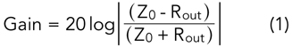
For this example, an American Microsemiconductor TD262A tunnel diode is measured as a function of frequency, as shown in Figure 2. The test fixture is shown in Figure 2a. The measurements (see Figure 2b) determine the required bias voltage to obtain the proper negative resistance.
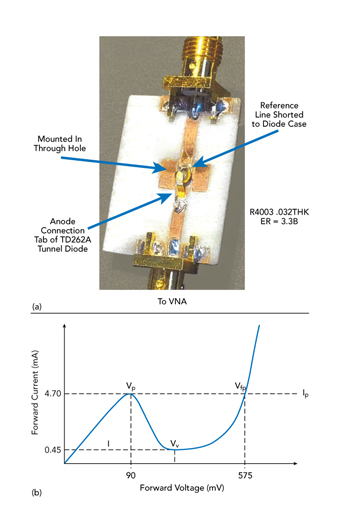
Figure 2 TD262A tunnel diode test fixture (a) and characteristic curve (b).
Figure 3 TD262A tunnel diode measured impedance.
A resistor is mounted in series with the diode such that the total resistance is positive, and impedance is measured using a VNA. A simple program subtracts the value of the series resistor and calculates the value of the real and imaginary parts of Zd (see Figure 3).
The equivalent circuit of a packaged tunnel diode is shown in Figure 4.8 The highest frequency at which there is negative resistance is constrained by the capacitance Cj, which for the TD262A is about 3.5 GHz. The TD262A is mounted in a low frequency package, which restricts this frequency. High frequency assembly and fixtures using chip and wire are required for operation at mmWave frequencies.
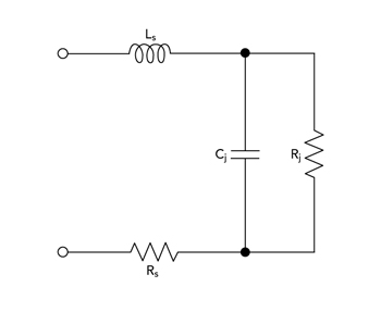
Figure 4 Packaged tunnel diode equivalent circuit.
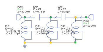
Figure 5 Butterworth bandpass filter schematic.
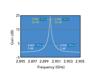
Figure 6 Gain versus frequency of negative resistance amplifier with Rsh = 100 Ω.
An amplifier with a gain of 25 dB is designed to operate at 2.9 GHz. It can be seen from Figure 3 that Rn equals -56.5 Ω and XCd equals -12.7 Ω. To resonate the diode at 2.9 GHz, Lsh is set to 0.237 nH. The bandpass filter is shown in Figure 5. It is a 10 percent bandwidth Butterworth filter centered at 2.9 GHz.
At 2.9 GHz, the resonant frequency of both the diode and the filter, the parallel combination of Rneg and Rsh must be equal to -44.68 Ω. The value of Rneg is given by Equation 2.
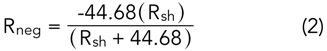
The computed gain versus frequency of the negative resistance amplifier shown in Figure 1, with a peak gain of 25 dB and Rsh equal to 100 Ω, is plotted in Figure 6. Rneg is found from Equation (2) to be -30.88 Ω, and since Rn equals - 56.5 Ω, Rser is set to 25.6 Ω.
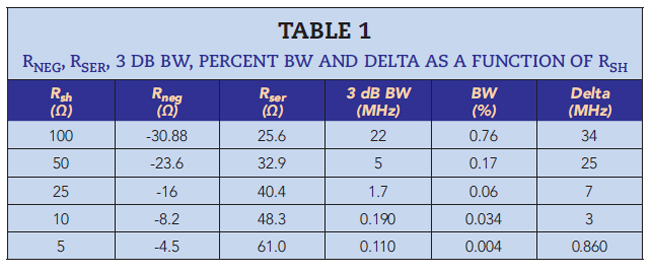
The 3 dB bandwidth is 22 MHz. Delta is the difference between the frequency at which the gain equals 3 dB and the center frequency of 2.9 GHz; this value is 34 MHz. In Table 1, Rneg, Rser, 3 dB bandwidth, percent bandwidth and Delta are tabulated for various values of Rsh. As can be seen from the table, percent bandwidths less than 0.004 percent are achievable.
CONCLUSION
A narrowband negative resistance amplifier is equivalent to a low noise amplifier followed by a narrowband filter. This filter can have bandwidths only achievable with superconductors. Grayzel1 presented the theory of the narrowband negative resistance amplifier, which was experimentally verified. In this article, the design of a narrowband negative resistance tunnel diode amplifier is presented and analyzed. It is shown that the bandwidth is a function of Rsh, the shunt resistor at the output of the negative resistance network and that percent bandwidths of less than 0.004 percent can be achieved. The circuits can be small and suitable for hand-held devices such as cell phones, as well as for miniature communication, telecommunication and defense receiver front ends.
ACKNOWLEDGMENT
The authors would like to thank Michael Hillbun, CTO of Diamond Engineering, for his contributions to the design and fabrication of the tunnel diode test fixture and for providing the measured data.
References
- “A Negative Resistance Amplifier with 0.5 Percent Bandwidth,” Microwave Journal, Vol. 66 No 5, May 2023, pp. 90–94.
- A. I. Grayzel and A. Gorwara, “Very Narrowband and Wideband Negative Resistance Amplifiers with a Tuneable Center Frequency Using a Coupler,” U.S. Patent 12 052 002 B2, July 30, 2024.
- A. I. Grayzel, “Very Narrowband and Wideband Negative Resistance Amplifiers with a Tunable Center Frequency,” U.S. Patent: US 11 863 131 B1, January 2, 2024.
- MQH-2R58R5CH MMIC 2.5-8.5 GHz Quadrature Coupler, Marki Microwave, Web: https://markimicrowave.com/products/bare-die/quad-hybrids/mqh-2r58r5ch/.
- Miniature Surface Mount 90-degree Hybrid Couplers, Innovative Power Products, Web: https://innovativepp.com/product-category/view-all-products/90-degree-hybrid-couplers/.
- Miniature 3 dB Hybrid Couplers, Mini-Circuits, Web: https://www.minicircuits.com/WebStore/90_180_degree_hybrid.html.
- F. Sterzer, “Tunnel Diode Devices,” Advances in Microwaves, Vol. 2, Edited by L. Young, Academic Press, 1967.
- Tunnel Diodes for Switching and Microwave Applications, RCA, 1963, p. 18.