Mobile data traffic continues to grow. Constant video streaming is on the rise in applications like TikTok, Netflix and Instagram, but also increasingly LinkedIn and even simple websites. Ericsson estimates that mobile data traffic, excluding fixed wireless access, is going to increase by a factor of 3x by 2029.1
While mobile traffic is expected to increase by multiples, revenues at mobile network operators are expected to stay flat. This is because the so-called “killer app” for 5G that helps to monetize new capabilities has not been found yet. This means customers continue paying the same for their 5G contract as they did for 4G.
This challenges network operators and radio manufacturers to manage a much higher data capability at the same total cost, which calls for a significant reduction in the cost per bit. This can be achieved by optimizing a multitude of levers. Combining frequency bands in one radio unit and employing wider frequency bands will reduce the number of required radios. Reducing the size and weight of radios will lower tower rental costs and reducing the consumed energy per radio will lower operators’ energy bills. Higher frequency bands need to be utilized, especially in high-density urban areas. To do this in a cost-efficient way, the grid of the radio base station ought not to be changed.2 This results in radios operating at 6 to 10 GHz, covering the same area as those operating at half that frequency. Finally, the cost of radio components is under pressure to lower initial capital expenditures.
Breaking these requirements down for 5G radios, the RF PAs need to support higher frequencies, significantly wider instantaneous bandwidths and high efficiency over a wide back-off range. These radios must also be capable of being linearized at levels below -50 dBc with digital predistortion (DPD). The semiconductor technologies capable of delivering those targets at a commercially viable price position are RF GaN-on-SiC and RF GaN-on-Si.
RF GAN-ON-SIC
Since the late 2010s, when the first 5G radios came on the market, GaN-on-SiC has increasingly been the semiconductor technology of choice for RF power amplifiers (PAs), increasing its market share to 51 percent of the current telecom market.3 First used for military and space applications where performance is the key driver, GaN-on-SiC has delivered the gain, power density and high transit frequency needed to power radar and communications from S-Band to Ka-Band. Wide telecommunications adoption has increased demand and volume. Many wafer fabs updated from 3 in. to 4 in. and, in some cases, 6 in. wafer manufacturing, driving down the initially high product cost of GaN-on-SiC wafers to levels more palatable for commercial applications.
New transistor concepts, like a graded AlGaN channel, were recently shown to improve power-added efficiency (PAE) and the linearity of GaN-on-SiC transistors at mmWave frequencies.4 A study5 used a sunken field plate to achieve higher voltage capability and gain while improving PAE. A paper6 introduced 0.25 μm RF GaN-on-SiC technology, reaching a maximum stable gain of 22 dB at 3.5 GHz and an fT of 23 GHz. The authors of that paper presented a Doherty demonstrator with greater than 16 dB gain that reaches between 49 and 55 percent efficiency for a W-CDMA signal between 3.4 and 3.8 GHz.
While the performance of RF GaN-on-SiC technologies will continue to improve, it is unclear how product prices will be significantly reduced. This price reduction is necessary to pave the way for fully integrated MMIC PAs to enable the best performance and commercial viability for massive MIMO (mMIMO) radios at 6 GHz and beyond. To focus the radio beam and create the same coverage range as a 3.5 GHz radio may require more than 500 antenna elements and 128 Tx channels in a 7 GHz radio.7 This means that the average PA price needs to come down.
RF GAN-ON-SI DEVICE-LEVEL PERFORMANCE
In November 2021, Infineon introduced its first generation of 28 V RF GaN-on-Si.8 The technology is used in RF PAs for 5G mMIMO base transceiver stations (BTS) and operates reliably in the field. Infineon introduced the second generation three years later. This new process is a fully MMIC-capable, 28 V, 0.25 μm RF GaN-on-Si technology manufactured on 8 in. wafers in an Infineon silicon fab.
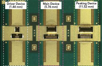
Figure 1 GaN-on-Si test cell.
RF GaN-on-Si uses a less expensive silicon substrate that is easier to procure than SiC substrates. Using 8 in. wafers drives the per-area cost down even more. This lower cost is expected to enable integrated RF PA architectures for frequencies greater than 6 GHz at a commercially viable price. RF GaN-on-Si can be produced in a silicon fab and does not need the separate manufacturing line typically required for RF GaN-on-SiC processes. The manufacturing equipment can be shared with other processes, allowing a more dynamic volume scaling. This helps reduce the volume dependency of manufacturing costs, enabling a reliable and sustainable manufacturing process throughout the market cycle. Manufacturing in a silicon fab involves the same tight process controls applied to other silicon processes, resulting in high process stability and low tolerances.
Infineon’s next-generation RF GaN-on-Si technology enables significant performance improvements, especially in gain. These improvements are made possible mainly by implementing a disruptive concept of advanced field-plate structures for the active devices. Compared to first-generation devices, this concept reduces parasitic feedback capacitances, Cdg. These transistors show better stability, 3 to 4 dB higher gain, lower frequency dispersion and more “Doherty-friendly” behavior, which is important to fulfill bandwidth and efficiency requirements for next-generation BTS deployments.
Figure 1 shows a test cell that will demonstrate the new technology’s device-level RF performance. The test cell contains different GaN-on-Si transistors with gate peripheries of 1.44 mm for a driver device, 5.76 mm for a main device and 11.52 mm for a peaking device. The gate pads of the transistors are wire-bonded to high Q metal-oxide-semiconductor capacitors (MOS caps) to provide low ohmic impedances for the second harmonics on the transistor input sides. The test cell is implemented on an 8 mm × 12 mm multi-layer laminate with identical dimensions, material and laminate layer stack-up to the one used for the Doherty PA module implementation described later. For this Doherty PA, only the main and peaking devices shown in Figure 1 are used; the driver device is prepared for future PA designs.
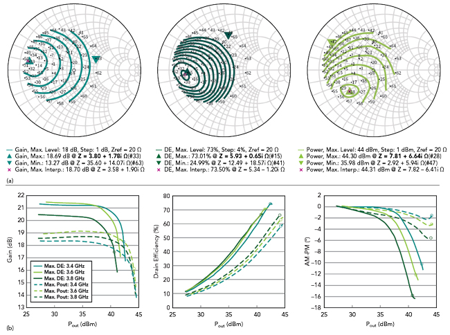
Figure 2 (a) Load-pull contours at 3 dB gain compression for the main amplifier at 3.6 GHz. (b) Power sweeps for the 5.76 mm main PA device.
Figure 2a shows the measured Smith chart load-pull contours for the 5.76 mm main PA device in Figure 1, with the 20 Ω taper de-embedded at 3.6 GHz for 3 dB transducer gain compression, drain efficiency and Pout, with 20 Ω reference impedances. The triangular markers in the plots show the load impedances and the corresponding minimum and maximum performance values. The load-pull measurements were performed at 28 V drain voltage and a quiescent current of 115 mA (20 mA/mm gate periphery), which was chosen to ensure a flat gain in power back-off. This performance is summarized in Table 1.

The solid curves of Figure 2b show the power sweeps for the ZLmax.DE = (5.3 - j1.2) Ω maximum drain efficiency load. The dashed curves show the sweeps for ZLmax.Pout = (7.8 - j6.4) Ω maximum output power load. These values have been optimized for 3.6 GHz, but the plots show 3.4, 3.6 and 3.8 GHz values.
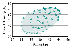
Figure 3 “Nose-plot” load-pull measurement results for the main device.
Figure 3 depicts the load-pull measurement data in a “nose plot,” which shows the drain efficiency versus Pout for all the applied load impedances in 3 dB gain compression at 3.6 GHz.
The performance of the driver and peaking devices of the test cells shown in Figure 1 is not explicitly shown in this article. However, it is close to the performance of the main device. The Pout performance scales according to the gate periphery of the device as compared to the 5.76 mm main transistor.
RF GAN-ON-SI DOHERTY PA MODULE
An 8 W (average) Doherty PA was designed with the main and peaking devices from the test cell shown in Figure 1 to operate over the 3.5 to 3.9 GHz frequency range. The PA, including an Infineon smart bias and control IC, was fabricated to be the same 8 mm × 12 mm size with the same multi-layer laminate as the device test cell. This enables using measured load-pull data and device models in the design and subsequent PA tuning. The peripheries for the main and peaking devices were chosen with a 1:2 ratio for optimum efficiency and linearity performance for 5G NR signals with 7.5 dB PAPR at 39 dBm Pout. The device output matching for the fundamental and second harmonics and the power combining network is accomplished with transmission lines on the laminate and high-quality SMD caps. The RF input signal separation for the main and peaking devices is implemented with a lumped-element 3 dB Wilkinson splitter. A smart bias and control IC is integrated into the module to control the biasing and TDD switching of the Doherty PA. This module is programmable with a digital I2C interface during the production cycle. This PA module is shown in Figure 4.
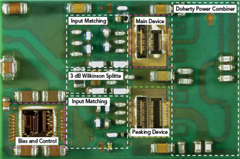
Figure 4 Doherty PA module with Infineon GaN-on-Si devices and bias and control IC.
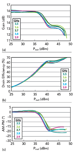
Figure 5 (a) Pulsed gain versus output power. (b) Pulsed drain efficiency versus output power. (c) Pulsed CW AM-PM versus output power.
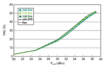
Figure 6 PAE versus average Pout.
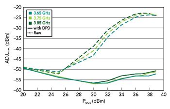
Figure 7 ADJmax versus average output power.
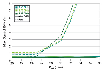
Figure 8 Maximum symbol EVM versus average Pout for 5G NR-TM3.1 test conditions.
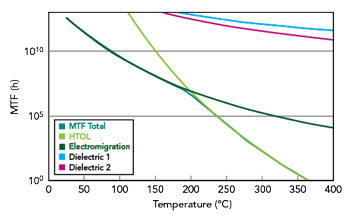
Figure 9 MTTF versus temperature for RF GaN-on-Si technology.
Figure 5a shows the gain performance, Figure 5b shows the drain efficiency and Figure 5c shows the measured AM-PM versus output power performance of the Doherty PA module shown in Figure 4. These results are measured with RF pulses having a pulse width of 200 μs and a duty cycle of 10 percent.
The gain of approximately 14.5 dB at 39 dBm average Pout, shown in Figure 5a, is close to the best values that have been published for GaN-on-SiC-based Doherty PAs with the drain voltage increased from 28 V to 50 V.6 The efficiency shown in Figure 5b is more than 55 percent at 39 dBm output power over 400 MHz bandwidth. Secondary research shows this is the same level as the best GaN-on-SiC Doherty PAs.6,9 The peak output power at 4 dB gain compression is greater than 47 dBm with a maximum AM-PM of 23 degrees, with about 6 degrees of phase variation over frequency at the average and peak power levels. The smooth gain and AM-PM behaviors shown in Figure 5a and Figure 5c are important for efficient wideband DPD linearization.
Figure 6 shows the measured modulated PAE versus output power for a 5G NR FDD signal with 256-QAM modulation, 1 × 100 MHz signal bandwidth, a signal carrier spacing of 30 kHz and PAPR = 7.5 dB for three different carrier frequencies. The dashed lines depict the non-linearized PAE curves and the solid lines show linearized performance with the DPD. At the average Pout of 39 dBm, the PAE value is greater than 50 percent.
The linearization performance in the frequency domain is evaluated with the adjacent channel power ratio as ADJmax = max [ADJleft, ADJright]. The results are shown in Figure 7 for different average power levels. At the 39 dBm Doherty PA average Pout, the linearized ADJmax is less than -51 dBc for a 100 MHz 5G NR signal with a PAPR of 7.5 dB. To assess the linearized performance in the time domain, the maximum symbol EVM versus output power must be considered for a 5G NR TDD test signal (NR-TM3.1) with 1 × 20 MHz signal bandwidth, a signal carrier spacing of 60 kHz and a PAPR of 8.4 dB. The measurement results in Figure 8 show an almost flat maximum symbol EVM of less than 1 percent over the PA linearized Pout.
RELIABILITY
Reliable device operation is a given. Devices in telecom infrastructure applications must typically operate for at least 10 years under harsh conditions. If devices can sustain higher temperatures, base station cooling facilities can be smaller and lighter, reducing operating costs for network providers. Figure 9 shows the MTTF of this new GaN-on-Si technology. For temperatures below 200°C, electromigration is the dominant failure mechanism. This failure is purely defined by the metallization layers of the process and the width of the connections and can be scaled independently of the intrinsic transistor. Above 200°C, intrinsic failure mechanisms of the transistors start to dominate. For a typical 150°C transistor operating temperature, the MTTF is 108 hours or 11,000 years, meeting lifetime requirements.
While there is no field data available yet for this second-generation technology, Infineon’s first generation of RF GaN-on-Si devices have been operating in the field in millions of PAs without any field returns, showing that RF GaN-on-Si is a suitable technology choice for harsh telecom applications.
SUPPLY VOLTAGE
The Infineon RF GaN-on-Si processes are developed for a supply voltage of 28 V and qualified up to 32 V. While the 8 to 12 W PAs commonly used in 5G mMIMO BTS can be designed with a 50 V supply, the slightly larger 28 V periphery and the lower output impedance allows for easier output matching. As base stations move toward frequencies above 6 GHz and the number of transmit channels increases, the average Pout of the PA will decrease. If the transformation ratio becomes too large, the impedance transformation networks and associated losses in the RF PAs become challenging and 28 V emerges as the sweet spot. For base stations operating at 10 GHz, with radios having 256 or more transmit channels, the industry is discussing even lower, 12 V, supply voltages. This will improve the competitiveness of GaN-on-Si even further.
CONCLUSION
The economic drivers of the BTS market that define current and future RF PA technical requirements are higher frequencies, wider instantaneous bandwidths and higher efficiency. Infineon’s second-generation RF GaN-on-Si technology provides a disruptive low feedback capacitance concept that significantly improves gain and “Doherty-friendly” PA behavior. The resulting Doherty PA has a PAE greater than 50 percent for a 100 MHz 5G NR signal at 39 dBm average output power. These results show the promise of this technology. The Doherty PA has been linearized to EVM values of less than 1 percent across the output power range from 3.6 to 3.8 GHz. With 8 in. silicon manufacturing and fabrication capabilities, the advantages of PA designs on RF GaN-on-Si technology will be apparent as higher frequencies for 5G Advanced and 6G emerge, requiring a commercially viable solution for MMIC integration.
References
- Ericsson, “Ericsson Mobility Report,” June 2024, Web: www.ericsson.com/en/reports-and-papers/mobility-report/reports/june-2024.
- Nokia, “Coverage evaluation of 7 - 15 GHz bands from existing sites,” White Paper, April 2024, Web: https://onestore.nokia.com/asset/213702.
- Yole Group, “RF GaN Compound Semiconductor Market Monitor Q2 2024,” 2024.
- J.-S. Moon et al., “Ultra-Linear and High-Efficiency GaN Technology for 5G and Beyond,” IEEE Topical Conference on RF/Microwave Power Amplifiers for Radio and Wireless Applications (PAWR), 2022.
- K. M. Bothe et al., “Improved X-Band Performance and Reliability of a GaN HEMT With Sunken Source Connected Field Plate Design,” IEEE Electron Device Letters, Vol. 43, No. 3, 2022.
- B. Grote et al., “High Performance 0.25 μm GaN Technology with Low Memory Effects,” BiCMOS and Compound Semiconductor Integrated Circuits and Technology Symposium, 2023.
- Ericsson, “Why cmWave spectrum is expected to be a powerful enabler of 6G and future networks,” 2023, Web: www.ericsson.com/en/blog/2023/6/cm-wave-spectrum-6g-potent-enabler.
- I. Nasr, “RF GaN on Silicon: The Best of Two Worlds,” Microwave Journal, Vol. 64, No. 11, Nov. 2021.
- S. Sakata et al., “A Fully-Integrated GaN Doherty Power Amplifier Module with a Compact Frequency-Dependent Compensation Circuit for 5G massive MIMO Base Stations,” IEEE International Microwave Symposium MTT-S, 2020.

