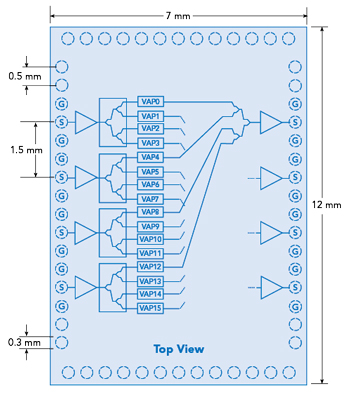
Figure 1 Block diagram of BFIC chip in a BGA package (not to scale).
Modern phased array systems are built using beamformer ICs (BFICs) that typically have multiple parallel paths on the chip with independently controllable gain and phase. Common BFIC configurations have two or more RF paths routed to pins on the same edge and/or the same corner of the IC package. Figure 1 shows a four-input, four-output, 16-channel BFIC with all four inputs on the same edge of the IC package. This device architecture is used on Analog Devices’ ADAR3000/1/6/7 family of Ku- and Ka-Band BFICs. Each device has four inputs, four cross-coupled outputs and a sophisticated digital control system that includes a command processor, on-chip RAM and FIFO memory.
The complexity and size of the BFIC creates challenges. The number of RF inputs and outputs and their associated ground-signal-ground configuration create close pin-to-pin placement. Routing multiple RF lines from these closely spaced pins to adjacent circuitry or other printed circuit boards (PCBs) is challenging. RF power tapering is widely used to reduce sidelobes, but since this can result in channel-to-channel power differences of up to 30 dB, channel-to-channel isolation is critical and the routing of RF lines can significantly impact isolation. In addition to routing issues, transmission line impedance is also very important. Poor transmission line impedance accuracy and poor impedance transitions between boards cause signal reflections and lower RF power delivery to the antenna. Large signal reflections can also cause instability and oscillation.
This article will discuss designing accurate RF PCB transmission lines with excellent return loss and isolation in dense, high channel count, multi-board environments. While we will focus on BFICs and phased array applications, the findings of this article apply equally to any high frequency circuit design where channel-to-channel isolation and good impedance matching are important. The article also covers the important topic of design for manufacturing.
RF TRANSMISSION LINE FABRICATION
PCB fabricators support multiple popular RF transmission line topologies, including microstrip, grounded coplanar waveguide (GCPW), stripline and the less popular buried GCPW, which resembles a hybrid of GCPW and stripline. While microstrip is relatively easy to manufacture, it is less popular for operation above 6 GHz because of its higher trace loss and poor mode suppression.1 GCPW, buried GCPW and stripline operate better above 6 GHz because of lower radiation loss and better mode suppression. Buried line topologies improve isolation but are more challenging to fabricate and require vias to connect to them. These vias are usually blind to minimize parasitic inductance, which results in higher board costs.
Figure 2 shows a cross-section of GCPW, buried GCPW and stripline, as well as the important geometries determining the nominal line impedance. These geometries are the line width (W1/W2/W3), the lateral distance from the edge of the line to the adjacent ground plane (G1/G2/G3), the thickness of the dielectric materials (T1/T2) and the relative permittivity of the dielectric materials ( εR1 / εR2 ). Figure 2 does not show the thickness of the copper used for the lines or the required ground via fencing. Copper thickness does need to be considered, but it is a secondary effect. Via fencing will be discussed later. The choice of topology depends on acceptable trace loss, frequency, required line-to-line isolation, available space and dielectric thickness of the PCB material.

Figure 2 Cross-section of GCPW, buried GCPW and stripline topologies.
HOW MANUFACTURING TOLERANCES AFFECTS LINE IMPEDANCE

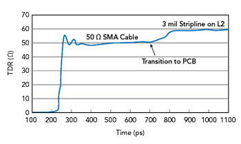
Figure 3 TDR plot of 3 mil wide stripline on Layer 2.

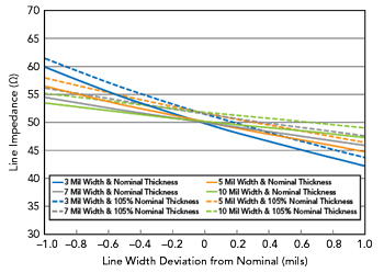
Figure 4 Line impedance versus line width deviation.
Fabrication tolerances affect the accuracy of RF line topologies. Figure 3 shows a time domain reflectometry (TDR) plot of a 3 mil wide stripline designed for 50 Ω but measured to be approximately 60 Ω. The initial target tolerance was ± 10 percent (45 to 55 Ω), yielding a return loss of more than 20 dB.
Many PCB fabricators offer trace widths down to 3 mil (copper weight is also a factor) with a 1 to 2 mil tolerance. 2,3,4 Dielectric manufacturers usually only provide typical dielectric thickness, most likely because the PCB fabricator determines the final thickness during the board lamination process. The lateral gap to the ground can vary if the ground plane does not stop where it should. In addition, the effective lateral gap width changes if the line width varies.
The lateral gap in microstrip and stripline RF traces is large by design and does not affect the line impedance. This results in all the field lines going to the lower ground plane for microstrip topologies and the upper and lower ground planes in stripline topologies. However, for a GCPW RF trace, the lateral gap-to-ground distance is relatively small by design, causing most of the field lines to go to the lateral ground plane.
Figure 4 plots the line impedance 5 of an RF stripline trace versus line width deviation from nominal. This is done for 3, 5, 7 and 10 mil nominal line widths. The plot also shows the impedance deviation when the dielectric is 5 percent thicker than the nominal value, assuming a stripline copper thickness of 0.7 mil and εR = 3.1.
Notice that the wider lines have less variance, while the impedance of the narrower lines varies more for the same absolute width deviation. Therefore, a wider nominal line width is more immune to fabrication variations. By contrast, when the dielectric thickness increases by 5 percent, the impedance shift is approximately equal, regardless of the nominal line widths. This means the PCB fabricator must meet the final pressed thickness requirements within a certain tolerance to attain the targeted line impedance tolerance. The focus in Figure 4 is on increased dielectric thickness because the observation over many PCB fabrication lots with different line topologies is that the line impedance tends to come out greater than or equal to the design target. This leads to a rule of thumb to design the line to be a few Ohms less than the target, especially when the width is thin (e.g., less than 5 mil). With this approach, the controlled impedance requirements that normally constrain the PCB fabricator may need to be waived. A reliable PCB fabricator should be chosen if a thin line must be used due to other design considerations. Confidence in PCB fabricators is established over time from multiple builds or by fabricating experimental boards with multiple lines of varying widths targeting 50 Ω ± 10 percent. Measurements would then be performed to determine which line width comes closest to 50 Ω.
GCPW VERSUS BURIED GCPW
On any PCB, two adjacent transmission lines will have some amount of coupling. This coupling can be electrical and/or through the electric and magnetic fields, resulting in non-infinite isolation. Poor isolation between transmission lines on a PCB is problematic, especially in applications with a significant difference in signal levels. In a phased array system using multichannel BFICs, parasitic signal coupling has been shown to degrade the linearity of the variable amplitude and phase (VAP) block’s gain control function in the high attenuation path when two adjacent channels are operating at minimum and maximum attenuation. This behavior was observed on an evaluation board with GCPW transmission lines. EM simulations with Keysight RFPro showed buried GCPW transmission lines improved in-band isolation between the lines by 15 dB versus the existing GCPW PCB solution.

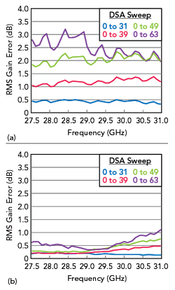
Figure 5 RMS Gain Error vs. Frequency over DSA settings for GCPW (a) and buried GCPW (b) transmission lines.
RMS gain error is an abstracted Figure of Merit indicator of gain control non-linearity. In this case, RMS gain error was measured on both versions of the PCB. Figure 5a shows the RMS gain error of the original PCB with GCPW, while Figure 5b shows the RMS gain error of the redesigned PCB containing buried GCPW. In Figure 5a, the RMS gain error is worst when the VAP block’s digital step attenuator (DSA) is exercised over its entire range. This is expected because the application is most susceptible to poor isolation when the delta between the DSA’s attenuation levels is at its largest. The higher line-to-line isolation of the buried GCPW board improved RMS gain errors significantly, aligning with simulations and displaying the actual performance of the BFIC. These results show that even a moderate improvement in isolation of 15 dB at 30 GHz can affect the measured performance dramatically.
