
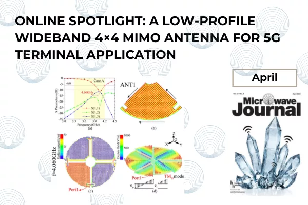
Figures 3b and c show the two-dimensional simulated vector current maps of Antenna 1 at 4.060 GHz. The black arrows in Figure 3b represent the current direction. From Figures 3b and c, it is apparent that resonance occurs in the ABD region (see Figure 2). The resonant mode for Case A corresponds to the fundamental TM11 mode of the quarter-circle patch. Figure 3d shows the three-dimensional vector electric field distribution of Antenna 1 below 4.060 GHz. The electric field changes from maximum to minimum along the angular direction, after which it flips and changes from minimum to maximum. The current gradually increases along the radial direction, consistent with the TM11 mode.
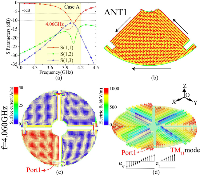
Figure 3 Case A – simulated S-parameters at Port 1 (a) simulated surface current distribution for Antenna 1 (b), simulated surface current distribution at Port 1 (c) and electric field distribution at 4.060 GHz.
Figure 4a shows the S-parameter plot for Case B. The center frequency is 3.844 GHz with – 6 dB points at 3.651 and 3.979 GHz. Figure 4b is the 2D current vector plot at 3.844 GHz that shows the resonant region confined within the shorting pins. The current direction flows from the middle to both sides, generating a resonant pattern like the TM1/2,1 mode of the half-mode patch.
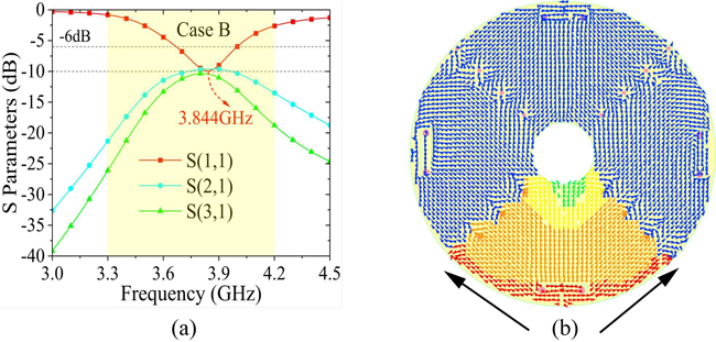
Figure 4 Case B – simulated S-parameters of Port 1 (a) and simulated surface current distribution of Port 1 at 3.844 GHz (b).
Case C adds the shorting pins to the conditions of Case A. This is the final structure. Since the shorting pins are placed along the zero point of the electric field in Case A, two different resonance modes are created when the pins are added. One is shown in Case A, where the basic mode of this circular patch antenna is TM1,1 mode. The other is a new TM1/2,1 resonant mode generated by the excitation of the shorting pins at 3.445 GHz (see Figure 5a).
The resonant frequencies are 3.445 and 4.046 GHz, and the – 6 dB impedance bandwidth covers the N77 band (3.3 to 4.2 GHz). By cutting out a circular slot in the middle of the antenna, isolation between diagonal elements is effectively increased.
Figures 5b and c show the two-dimensional vector current diagram of Antenna 1 at 3.445 GHz. Its resonant mode is stimulated with the shorting pins. The current direction within the fan patch flows from the edges of the shorting pins, which is because the pins divide it into the main patch and the parasitic patch. From the three-dimensional vector electric field distribution in Figure 5d, it is apparent that the antenna generates a pair of mirror TM1/2,1 resonant modes at 3.445 GHz.
Figure 5 Case C – simulated S-parameters of Port 1 (a), simulated surface current distribution of Antenna 1 (b), simulated surface current distribution of Port 1 (c) and electric field distribution at 3.445 GHz (d).
At 4.046 GHz a three-eighth circular resonant patch is formed (see Figure 6). It is the resonant mode generated by Cases A and B together. The antenna generates two resonant modes, namely the TM11 mode and the TM1/2,1 mode. Note that the design adopts a microstrip line for coupled feeding. The microstrip line is used to connect antenna 1 and antenna 2.
As seen from the two-dimensional vector current diagram, the joint excitation of antennas 1 and 2 generates the resonant mode. The resonant TM1,1 mode is generated in antenna 1 due to the fundamental pattern produced by the quarter circular patch in Case A, while the resonant TM1/2,1 mode is generated in antenna 2. This is because of the half-mode patch TM1/2,1 mode from Case B due to the shorting pins.
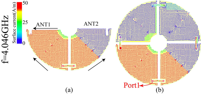
Figure 6 Simulated surface current distribution of Antenna 1 (a) and Port 1 (b) at 4.046 GHz.
RESULTS AND DISCUSSION
To verify the antenna design, a prototype is built and tested (see Figure 7). Due to welding errors, the difficulty in maintaining a 2 mm air layer and the relative flatness of the 0.4 mm dielectric substrate, there are some differences between measurement and simulation, but these differences are not substantial.
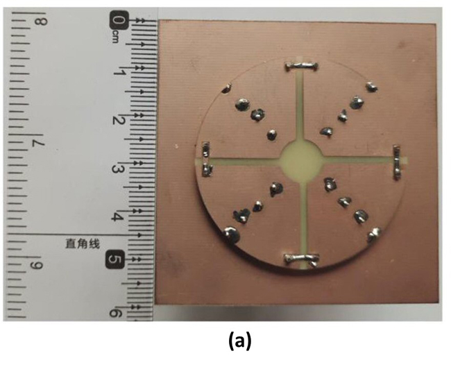
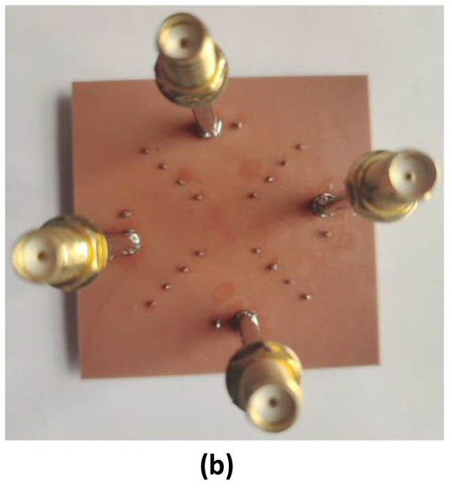
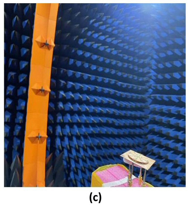
Figure 7 Fabricated prototype: top view (a), bottom view (b) and the antenna mounted in an anechoic chamber for testing (c).
Figure 8 shows the S-parameters, total efficiency and the envelope correlation coefficient (ECC) of the antenna simulation. From the S11 plot, the antenna's simulated – 6 dB impedance bandwidth is 900 MHz (3.30 to 4.20 GHz) providing coverage of the newly introduced N77 5G band (3.30 to 4.20 GHz). Isolation between adjacent and diagonal antenna elements is flat, and greater than 10 dB.
The range of total efficiency within the N77 band is 38 to 68 percent. Because the antenna is arrayed in a rotated grid and the elements are orthogonally polarized, the ECC is relatively small at less than 0.25 across the band.
Figure 9 shows the measured results. It is consistent with the simulations. At – 6 dB, the measured impedance bandwidth is slightly less than the simulated value, and isolation at greater than 10 dB is consistent with simulated results. The antenna efficiency is between 35 and 70 percent and the ECC is lower than 0.26.
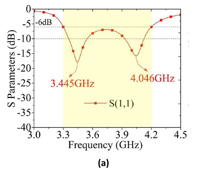
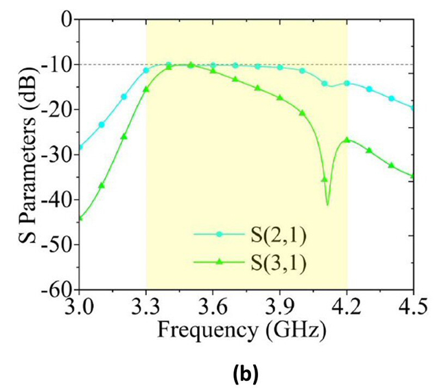
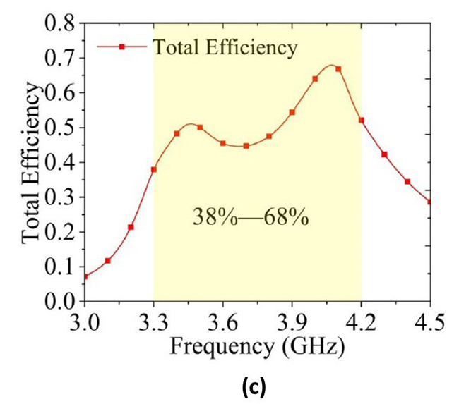
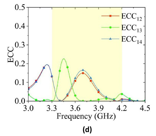
Figure 8 Simulated antenna reflection coefficient (a), mutual coupling (b), efficiency (c) and ECC (d).
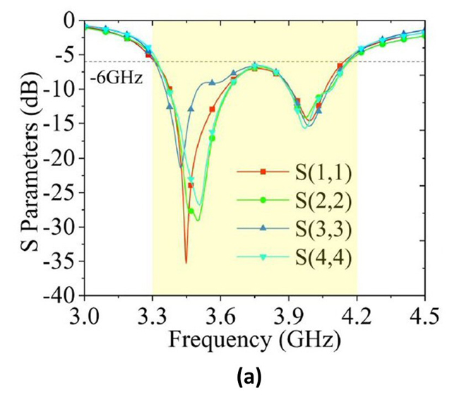
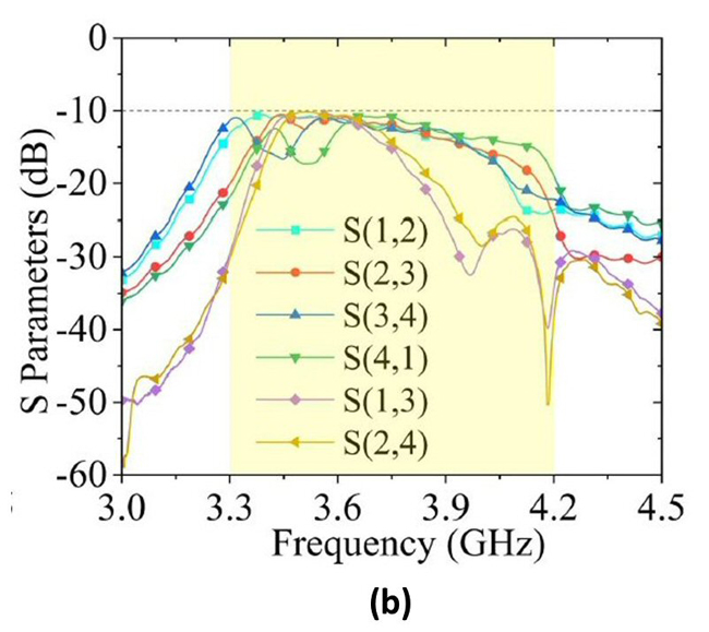
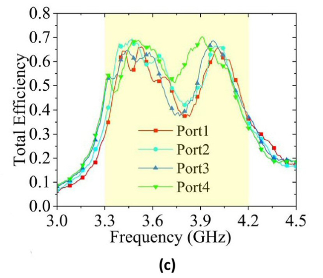
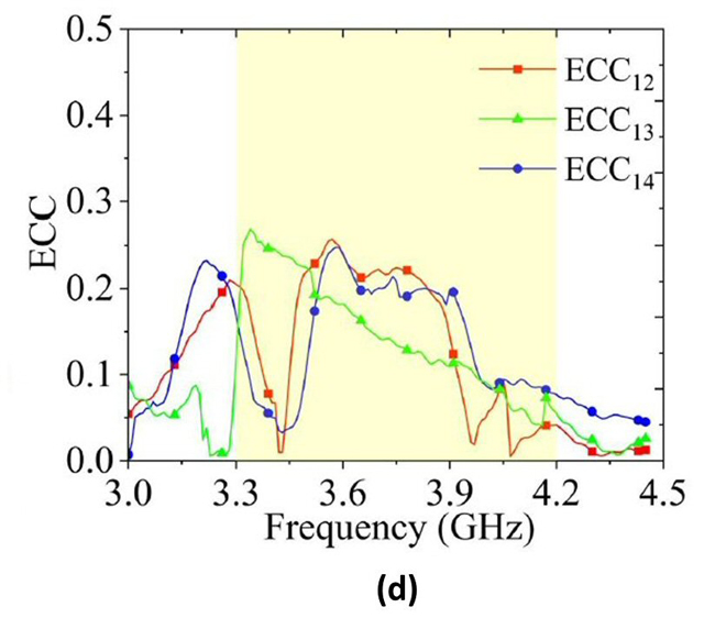
Figure 9 Colosseum block diagram.Measured antenna reflection coefficient (a), mutual coupling (b), efficiency (c) and ECC (d).