
Density, both informational and physical, determines complex RF system success or failure. Systems like 5G and Wi-Fi 7 pack more information into precious spectrum on smaller base stations, access points and devices. Finding density-related problems at prototyping, or later in deployment, adds cost and risk. Traditional RF electronic design automation (RF EDA) workflows are falling behind density challenges, analyzing one problem at a time and missing too much. A new approach: solving electromagnetic (EM) densification at the point of design.
Shift left—earlier visibility on designs in virtual space is the fundamental purpose of EDA tools. When modeling and simulation reflect real-world performance, design problems become easier to fix. Still, complex densification problems have many domains with combined interacting effects. Pulling EDA and test and measurement tools together in a workflow knocks out EM problems earlier, before committing to hardware. This article reviews three examples regarding how these workflows are solving EM densification:
1. Analyzing wideband designs using modulated signals and authentic waveforms1
2. Visualizing stability with EM-circuit excitation early in design and physical layout2
3. Increasing confidence in EM design integrity through iterative co-simulation.3
EM workflows appear across the ecosystem, soon connecting vendors, customers and customers-of-customers through “simulatable datasheets,” which is briefly explained.
TAKING ON INFORMATION DENSITY
Wireless systems broke free of some limits, but moving information still has boundaries. When Claude Elwood Shannon explored communication channels, he saw their data capacity maximized by bandwidth, using signals with many noise-like characteristics. Analog systems with inefficient modulation left data-hungry services unsatisfied. Digital systems packed more bits into each transmitted symbol, saving bandwidth, but true to Shannon, complexity rose and specifications tightened.
Today, complex modulations are part and parcel of RF system specifications including 5G and Wi-Fi 7. Digital quadrature amplitude modulation (QAM) arranges data points in a two-dimensional constellation. Higher-order constellations put points closer together, requiring a higher signal-to-noise ratio to keep error rates down. 5G new radio (NR) features 256-QAM modulation delivering eight bits per symbol. Wi-Fi 7 is moving to 4096-QAM modulation for 12 bits per symbol. Orthogonal frequency division multiplexing bundles dense carrier sets into a narrow bandwidth leading to sudden intense peaks, as much as 10x the average power level, creating dramatic noise-like stresses on radio architectures. Both 5G and Wi-Fi 7 add MIMO antenna technology and spatial multiplexing for increased throughput within a given bandwidth.
In this light, error vector magnitude (EVM) emerges as a critical metric for signal quality and for transceiver and equipment performance. It is an RF designer’s proxy for bringing the customer experience forward to the point of design. EVM measures how accurately transmitted symbols match their intended spot in the QAM constellation (see Figure 1). Higher-order QAM constellations put points close together to start. Imperfections in a radio shift constellation points off their mark. These effects include non-linearity, noise, loading and channel interference. When points are close together, accurate discrimination between adjacent points becomes harder.
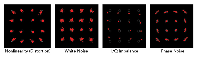
Figure 1 EVM impairments and symbol errors in a 16-QAM constellation.
All this leads to an observation. It is not possible to design a 5G NR or Wi-Fi 7 compliant radio without incorporating a higher-order modulation scheme per specification. To prove such a transmitter works, authentic higher-order modulated signals of sufficiently wide bandwidths are required to measure EVM performance at system validation. In fact, every modern digital RF system relies on complex modulation for achieving its desired information density. For these systems, there is no such thing as a choose your own compliance adventure.
Yet, that is exactly how many designers pursue physical design densification. At the point of design, EDA tools perform schematic capture, physical layout and localized simulations of design choices. Are those choices understood in a system context? Does optimizing one factor have consequences on others? Is it possible to tell what those interrelationships might be? Simulating approximate or incomplete models with simplified signals looking for one problem is an excellent way to miss others.
Those mysteries lead teams to fall back on physical prototypes for observing and troubleshooting RF issues. Hardware re-spins, however, are expensive schedule killers. Anything from functional design errors to hard-to-reproduce interactions under dynamic conditions can trigger a re-spin. Waiting until prototyping to find any lurking issue leaves RF designers at the mercy of higher risks and project costs.
Let us return to the EVM example and look at why modulated signals are important for accurately characterizing power amplifiers (PAs). S-parameters and pure sinusoidal stimuli provide a modeling baseline of raw PA performance. The same PA in a hardware prototype running against complex modulation may fall apart in unexpected ways. Why? Combining physical densification, power, modulated signals and a host of parasitic effects pushes assumptions, exposing various design weaknesses.
Effects factoring into EVM spread across domains in two categories as shown in Figure 2. Quickly varying effects are waveform-related and are how information density shows up. Besides power effects, demanding signals bring implications in both frequency and time domains. Slowly varying effects impact a device’s operating point and are often byproducts of physical density. Thermal, load and bias dependence reveal issues with stability, coupling, resonances, frequency shifts, matching and package interactions.
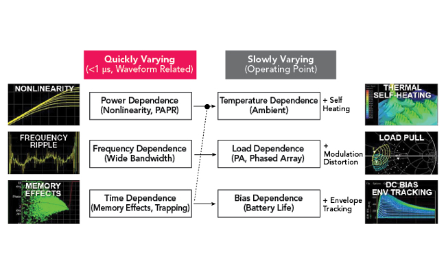
Figure 2 Factors affecting PA performance and EVM.
These effects are not entirely separable. A complex waveform can set off time-dependent memory effects such as charge trapping and self-heating. Sweeping frequency across a wide bandwidth finds linear impedance mismatches and ripple varying across the band. However, a wide bandwidth waveform excites all factors simultaneously, creating “rogue waves” with infrequent and sudden signal peaks 8 to 13 dB above the average power level. Under extreme peak-to-average power ratio conditions in regulated frequency bands, PA energy efficiency, signal quality and output power become harder to optimize. Modulated waveforms with accurate carrier dynamics uncover more issues than one-tone and two-tone analyses using harmonic balance.
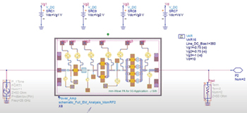
Figure 3 5G mmWave PA design using PathWave Advanced Design System.
This highlights the risk of waiting until hardware prototyping before fully exercising RF designs. Staging physical effects in combination may also be exceedingly difficult, which leads to latent problems cropping up in system deployment. In virtual space, simulators can sweep combinations of parameters in the presence of authentic wideband signals; but higher bandwidth signals also force more data collection, slowing the characterization process.
For increased test coverage of parametric scans, intelligent test and measurement trade-offs on signal complexity reduce measurement time with techniques like signal compaction and modulation distortion (or distortion EVM). These same techniques can apply to simulations, along with intelligent trade-offs for accelerating RF characterization without sacrificing fidelity. An example is fast circuit envelope technology in EM co-simulations, capturing linear frequency responses, loading, power dynamics and bias effects and even memory effects in a run-time, on-the-fly modeling step.
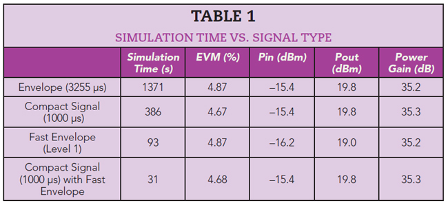
Figure 3 shows a mmWave PA design and Table 1 shows the PA simulation results from 50,000 points of a 5G modulated source. Applying both compact test signals and fast envelope techniques improves simulation time by 44x with little change in EVM accuracy. This increase in speed is critical to gaining design insights. It is the difference between simulating an EVM test case once at verification versus simulating EVM contours against a parametric scan and making incremental design improvements.
This two-way workflow between RF EDA and test and measurement algorithms enables designers to probe deeper much earlier, handle changes at the point of design and achieve consistency with measured results. Dense systems can be created, simulated, adjusted and re-simulated with authentic signals and combinations of effects modeled. Margins against system-level metrics are no longer a guess.
Modulated signals also enable the system experience to travel up and down the ecosystem. Understanding performance in a customer’s environment is key to achieving information density goals. Next is a look at a deeper example where physical density sets up complex EM interactions.
ONE-PASS STABILITY ANALYSIS
Amplifier instability occurs when gain and feedback mix. With frequencies, bandwidths, complexity and physical density rising, resonances are now common. Bypass capacitors may be a fix. Compact packaging makes placing capacitors hard, and where and how much capacitance to use is unclear.