
The MMIC was fabricated with a selective epitaxial growth technique on GaAs substrates. The optimized PIN diode epitaxial structure was grown first, followed by definition of the PIN diode and PHEMT active regions. A second epitaxial growth of PHEMT material followed, and the complete PIN-PHEMT process merged the 0.15 μm PHEMT and PIN processes, with base mesa and p-ohmic steps used to create the limiters. Mesa isolation was performed using wet chemical etching, and the T-shaped PHEMT gate was defined using electron beam lithography. Air bridges formed the on-chip inductors and interconnected the PIN diodes and other devices.
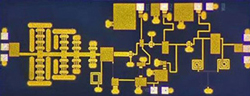
Figure 4 Fabricated PIN diode limiter-LNA MMIC.
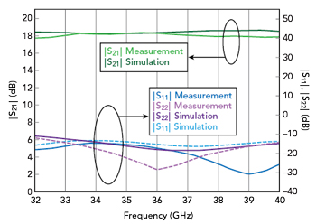
Figure 5 Simulated vs. measured small-signal performance.
MEASUREMENT AND ANALYSIS
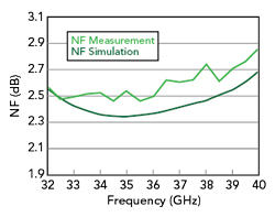
Figure 6 Simulated vs. measured NF.
The fabricated limiter-LNA MMIC is shown in Figure 4. S-parameters and NF were measured on-wafer at room temperature, with the amplifier biased at VG1 = VG2 = -0.4 V and VD1 = VD2 = 2 V. The current consumption of the entire MMIC was 36 mA, with a power dissipation of 72 mW. Figures 5 and 6 compare the measured and simulated gain and NF performance of the limiter-LNA. From 32 to 40 GHz, the measured average small-signal gain was 18 dB with a gain flatness of ±0.4 dB. |S11| and |S22| were better than -14 dB and -12 dB, respectively. The measured NF ranged from 2.5 to 2.9 dB across the full band.
To measure the power handling capability of the limiter-LNA, the die was attached using AuSn solder to a copper-molly carrier, which provided maximum heat conduction. The input power was increased from -30 dBm, measuring the S-parameters and NF before and after 30 minutes of exposure. The limiter-LNA handled up to 39 dBm of CW input power at 36 GHz without failure.
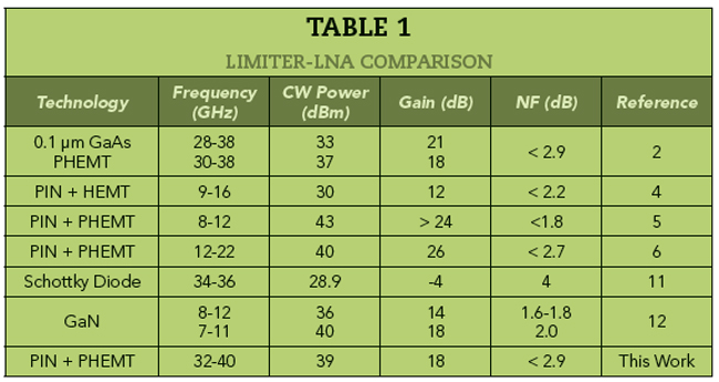
A comparison of this limiter-LNA with similar work is provided in Table 1. Compared with other reported Ka-Band PIN diode limiter-LNAs, this limiter-LNA design achieved the highest power handling capability with comparable performance.
CONCLUSION
A 32 to 40 GHz high-power GaAs PIN diode limiter-LNA MMIC has been described. The PIN diode limiter network forms a lowpass filter which serves as an input matching circuit for the LNA. CW input power handling was 39 dBm, the overall NF less than 2.9 dB with 18 dB small-signal gain over the 32 to 40 GHz band. The RF power handling was greater than that of typical Schottky diode limiter-LNAs because of the power handling capability of PIN diodes. This demonstrates the potential of PIN diode limiter-LNAs for mmWave front-end circuits.7
ACKNOWLEDGMENT
This research was funded by the National Natural Science Foundation of China (61774054).
References
- I. J. Bahl, “10 W CW Broadband Balanced Limiter/LNA Fabricated Using MSAG MESFET Process,” International Journal of RF and Microwave Computer-Aided Engineering, Vol. 13, No. 2, February 2003, pp. 118–127.
- P. Mahmoudidaryan and A. Medi, “Codesign of Ka-Band Integrated Limiter and Low Noise Amplifier,” IEEE Transactions on Microwave Theory and Techniques, Vol. 64, No. 9, September 2016, pp. 2843–2852.
- N. Billström, M. Nilsson and K. Estmer, “GaAs MMIC Integrated Diode Limiters,” Proceedings of the 5th European Microwave Integrated Circuits Conference, September 2010, pp. 126–129.
- P. Huang, W. L. Jones, A. Oki, D. Streit, W. Yamasaki, P. Liu, S. Bui and B. Nelson, “A 9-16 GHz Monolithic HEMT Low Noise Amplifier with Embedded Limiters,” Proceedings of the IEEE MTT-S International Microwave Symposium, May 1995, pp. 205–206.
- X. Zhou, Y. Li, G. Zhou, H. Wei, X. Gao and H. Wu, “Design of X-Band Miniature Balanced Limiter-Low Noise Amplifier Chip,” Proceedings of the International Conference on Microwave and Millimeter Wave Technology, May 2018.
- L. Cui, X. Zhou, Y. P. Li and H. T. Wei, “Codesign of 12-22 GHz Integrated PIN-Diode Limiter and Low Noise Amplifier,” Proceedings of the 14th IEEE International Conference on Solid-State Integrated Circuit Technology, November 2018.
- L. Yang, L. A. Yang, T. Rong, Y. Li, Z. Jin and Y. Hao, “Codesign of Ka-Band Integrated GaAs PIN Diodes Limiter and Low Noise Amplifier,” IEEE Access, June 2019.
- S. S. Yang, T. Y. Kim, D. K. Kong, S. S. Kim and K. W. Yeom, “A Novel Analysis of a Ku-Band Planar PIN Diode Limiter,” IEEE Transactions on Microwave Theory and Techniques, Vol. 57. No. 6, June 2009, pp. 1447–1460.
- J. M. Carroll, “Performance Comparison of Single and Dual Stage MMIC Limiters,” IEEE MTT-S International Microwave Symposium Digest, May 2001, pp. 1341–1344.
- L. Pace, S. Colangeli, W. Ciccognani, P. E. Longhi, E. Limiti, R. Leblanc, M. Feudale and F. Vitobello, “Design and Validation of 100 nm GaN-on-Si Ka-Band LNA Based on Custom Noise and Small Signal Models,” Electronics, Vol. 9, No. 1, January 2020.
- L. Z. Yang, H. Q. Hu and J. Xu, “Ka-Band Schottky Diode Limiter,” International Conference on Computational Problem-Solving, October 2011.
- P. Schuh and R. Reber, “Robust X-Band Low Noise Limiting Amplifiers,” IEEE MTT-S International Microwave Symposium, June 2013.