
This article describes a novel 32 to 40 GHz high-power GaAs PIN diode limiter and low noise amplifier (limiter-LNA) MMIC. To improve small-signal performance and reduce chip area, a unit cell comprises the PIN diodes and matching inductor, and the unit cells are cascaded to match the input of the LNA. The limiter-LNA handles up to 39 dBm CW input power without failure. Small-signal gain and noise figure (NF) were 18 ±0.4 dB and 2.5 to 2.9 dB, respectively, over the 32 to 40 GHz frequency range.
Advancements in wireless communication technology have increased the demand for mmWave integrated circuits. The LNA is a key component of the receiver and must have high gain and low NF. LNAs are typically the first block in a receiver; however, their power handling capabilities are only 10 to 20 dBm CW.1 Limiters are used to protect these sensitive LNAs with, ideally, sufficiently low levels of leakage power and minimal signal loss and distortion. Traditionally, LNAs and limiters have been designed independently with 50 Ω input and output matching networks, which occupy a relatively large area and add insertion loss, especially in the mmWave band. By integrating the limiter and the LNA into a single chip, circuit real estate is reduced and better performance is achieved by eliminating external connections.2
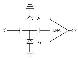
Figure 1 PIN diode limiter-LNA topology.
Schottky diode limiter-LNAs are widely used;1,2 however, they have relatively low power handling capabilities.3 Compared with Schottky diode limiters, PIN diode limiters have relatively high power handling capability; thus, an integrated PIN diode limiter-LNA MMIC offers the advantages of small size and high power handling. Jones et al.4 demonstrated a 9 to 16 GHz PIN diode limiter-LNA with 12 dB of gain and less than 2.2 dB NF with 30 dBm CW input power handling. Zhou et al.5 describe an X-Band balanced PIN diode-based limiter-LNA with a power handling capability of 20 W CW, where the limiter-LNA had 24 dB gain and less than 1.8 dB NF across the 8 to 12 GHz band. Cui et al.6 describe a 12 to 22 GHz, 10 W PIN diode-based limiter-LNA with a small-signal gain of 26 dB.
In this work, a 32 to 40 GHz high-power monolithic integrated PIN diode limiter-LNA was designed with combined PIN diode and PHEMT technology. To improve small-signal performance and reduce the chip area, the PIN diode limiter network was designed to be the LNA’s input matching circuit. The 0.15 μm gate length GaAs PHEMT and the PIN diodes were epitaxially grown and processed on the same wafer. Measurements show the PIN diode-based limiter-LNA is capable of handling 39 dBm CW input power without failure, achieving 18 dB average small-signal gain and 2.5 to 2.9 dB NF over the 32 to 40 GHz band.
DESIGN AND FABRICATION
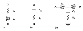
Figure 2 Equivalent circuit of the PIN diode with high input power (a), low level input (b) and tuning the diode capacitance (c).
Concurrent design of the limiter and LNA was the source of improved performance, as the output impedance of the limiter was directly matched to the input impedance of the LNA, eliminating the 50 Ω matching networks typically used between the limiter and the LNA.3 Figure 1 shows the basic topology.
With a high-power input signal, the PIN diodes, D1 and D2, turn on, the antiparallel diodes clipping both halves of the sinusoidal RF signal to limit the input voltage to a safe value. A significant fraction of the incident power reflects to the source. The PIN diodes absorb some of the input power, as well, decreasing the output power. With a low-power input signal, the diodes are “off” and load the RF path with parasitics.7
With a high-power input, the PIN diode junction capacitance is essentially shorted (see Figure 2a), and the conducting RF resistance is about 1 Ω, due to the increased density of charge carriers in the semiconductor. For small-signal levels, the equivalent circuit of the PIN diode can be approximated by CR in series with RS8 (see Figure 2b). The insertion loss caused by CR can be addressed with impedance matching: the series inductor, Lb, added to the limiter network to compensate (see Figure 2c).
The PIN diodes, with their shunt capacitance, and the matching inductors compose a unit cell. The unit cells are cascaded to form a lowpass filter to provide input matching to the LNA, improving its noise performance. Transmission lines are employed in each cell, their length and impedance optimized to realize the series inductor Lb.
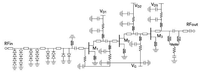
Figure 3 PIN diode limiter-LNA MMIC schematic.
The integrated four-stage PIN diode-based limiter and three-stage LNA were designed and implemented using a process offering both PIN diodes and 0.15 μm PHEMTs. Figure 3 shows the schematic of the limiter-LNA MMIC. The antiparallel diode structure maximizes power handling and, by double stacking the diodes, the shunt capacitance was reduced by 2x. An RF choke inductance shunted to ground provides a DC return path for the limiter.9 In the LNA network, inductive source degeneration10 improves both the noise performance and input matching. An equalizer consisting of series inductors, resistors and a capacitor helps flatten the gain by decreasing the low frequency gain, as well as improving circuit stability.