
Decades of research and development dedicated to GaN RF power semiconductor technology has led to an increasing supply of affordable RF power devices with impressive performance. GaN semiconductors have reduced material capacitance and enhanced electron mobility, resulting in remarkably low conduction losses, considerably faster switching times and higher frequency-temperature and frequency-voltage characteristics than silicon technologies. Extensive lab testing conducted by numerous sources consistently demonstrates these performance advantages over competing technologies, which has hastened the deployment of GaN power devices in numerous applications. Now, design engineers worldwide are harnessing these compact, low loss and fast switching semiconductors to develop smaller, lighter and more reliable systems that extend the capabilities of solid-state RF power design.
With the many benefits of GaN come a set of challenges with new circuit designs. For example, passive components at the output of a GaN device can reduce the output power of the active component. Even if the passive components don’t introduce excessive loss, they can degrade GaN’s ability to operate at maximum performance. Some of these design challenges can be overcome by using high performance passive components, such as advanced capacitors and surface-mount technology (SMT) heat pipes. This symbiotic relationship between passive components and GaN RF power devices makes the capacitor selection process critical.
This article addresses several high performance passive component technologies that pair well with GaN to provide impedance matching, bias filtering, DC blocking and thermal control, helping GaN power devices operate optimally.
SINGLE-LAYER CAPACITORS AND IMPEDANCE MATCHING
Single-layer capacitors (SLC) are comprised of a single ceramic dielectric layer with terminations for conductive epoxy attachment and wire bonding. Providing good performance through 40 GHz, they can be used in internal and external configurations—for example, playing an integral role in maximizing the power transfer of a GaN power amplifier as part of the impedance matching networks. When placed inside a device package, SLCs can be elements of a matching network between the lead frame and gate of the transistor, helping provide a broadband impedance match at the input of the device. Used outside the package, SLCs can be used for impedance matching, DC blocking and broadband bypassing. SLCs can be configured as single, dual or multiple SLC arrays to minimize component count.
Most of the electrical characteristics of SLCs are determined by the ceramic dielectric used for their construction. The two most common dielectrics are SiO2 and C0G (NP0) EIA Class I temperature-compensating ceramic. Both have high temperature stability (0 ±30 ppm/°C), ideal for impedance matching where temperatures are high and thermal stability is critical. A new type of dielectric, the grain boundary barrier layer (GBBL) material system, has demonstrated noteworthy performance as a replacement for the general-purpose Z5U and Y5V ceramic dielectrics where bulk capacitance is a concern. A typical GBBL dielectric exhibits X7S temperature characteristics with better temperature stability compared to the Z5U and Y5V dielectrics (see Figure 1).
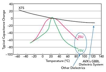
Figure 1 Temperature stability of Z5U, Y5V and X7S dielectrics. The GBBL material system has X7S temperature characteristics.
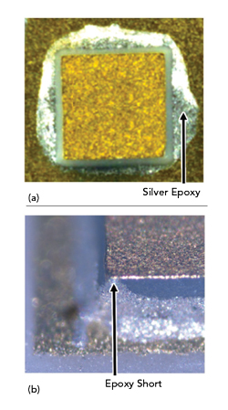
Figure 2 Bordered (a) and non-bordered (b) SLCs. Excess conductive epoxy can climb up the sidewall of a non-bordered SLC and cause a short. Source: TJ Green Associates, LLC.1
SLC terminations are typically comprised of sputtered TiW/Au or TiW/Ni/Au. This combination of sputtered materials yields thin, high-quality termination surfaces with excellent adhesion, essential for conductive epoxy attachment and wire bonding, particularly with high-power RF devices subject to severe temperature cycling. The terminations can be bordered, which means the metallization does not extend to the capacitor edges, or non-bordered, which means it does (see Figure 2). Bordered SLCs minimize the chance of conductive epoxy climbing the sidewalls to touch the top plate and short the capacitor. Ideally, epoxy fillets should flow about halfway up the side of an SLC, but since MIL-SPEC requirements don’t specifically specify conductive epoxy fillet height on die edges, using bordered SLCs can avoid the possible negative outcome from overflow.1 Non-bordered SLCs are typically used in source bypass configurations because they reduce the bond length between the top termination and the active device.
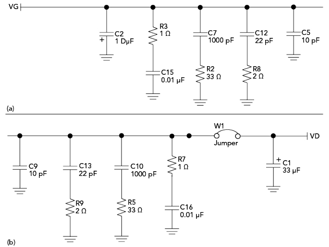
Figure 3 Gate (a) and drain (b) bias filter banks. Source: Qorvo.2
BULK CAPACITORS FOR BIAS FILTERING
GaN power devices require a stable bias voltage for optimum operation. Since bulk capacitor banks are stable with voltage and temperature and have good aging characteristics, they are often used to filter bias line noise and provide a fast source of charge to supply the high current changes (Δi/Δt) in a power amplifier (see Figure 3). The transient response of these filter capacitor banks is determined by the combination of high capacitance and high frequency response. Bulk capacitors suitable for voltage bias banks include high-CV multilayered ceramic capacitors (MLCC) and tantalum, tantalum-polymer, aluminum and aluminum-polymer electrolytic capacitors (see Figure 4).
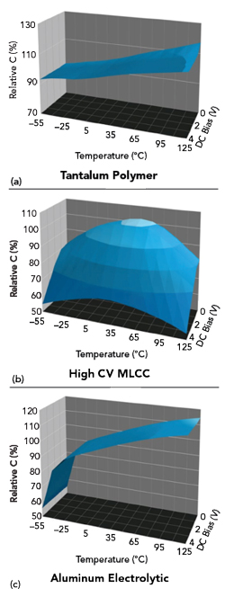
Figure 4 Capacitance stability, DC bias and temperature performance for tantalum polymer (a), high-CV MLCC (b) and aluminum electrolytic (c) capacitors.
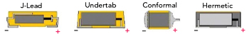
Figure 5 Tantalum capacitor packaging options.
While high-CV MLCCs can achieve the capacitance ranges required for many bias networks, they don’t provide stable capacitance values across operating conditions such as temperature, time and DC bias.3 For example, the capacitance stability of a 100 μF X5R MLCC can vary from 100 μF at 25°C to approximately 85 μF at -55°C and 80 μF at 125°C. High-CV MLCCs also suffer from DC bias voltage effects that can significantly reduce the capacitance value present in the circuit. For example, the capacitance value of a Class II MLCC can decrease by 35 to 65 percent at the fully rated DC current. Additionally, low voltage AC ripple current can further reduce the capacitance of high-CV MLCCs by another 5 percent, and aging can reduce the capacitance by another 2 to 5 percent per decade. Depending on the operating conditions and the MLCC chosen, all these losses combined with the temperature coefficient can reduce the total expected capacitance of high-CV MLCCs by approximately 80 percent.
The remaining bulk capacitor options suitable for bias filtering include traditional and polymer versions of tantalum and aluminum electrolytic capacitors. Although this article focuses on tantalum bulk capacitors for bias filtering, aluminum capacitor technology and performance are also improving. Tantalum capacitors have size, weight and stability advantages over traditional aluminum electrolytic capacitors. For example, tantalum capacitors have an average capacitance of 0.6 μF/mm3 compared to miniature aluminum electrolytic capacitors, which have an average capacitance of 0.1 μF/mm3. Tantalum-polymer capacitors exhibit approximately one-eighth the equivalent series resistance of traditional tantalum capacitors, meaning a current capacity approximately 8× of traditional tantalum capacitors. Advances in tantalum-polymer capacitor technologies have also extended the voltage rating of miniature SMT capacitors to 125 V. While traditional tantalum capacitors require 50 percent derating, tantalum-polymer capacitors rated up to 16 V only require 10 percent derating for polymer substrate devices and 20 percent derating for those rated for greater than 16 V operation.
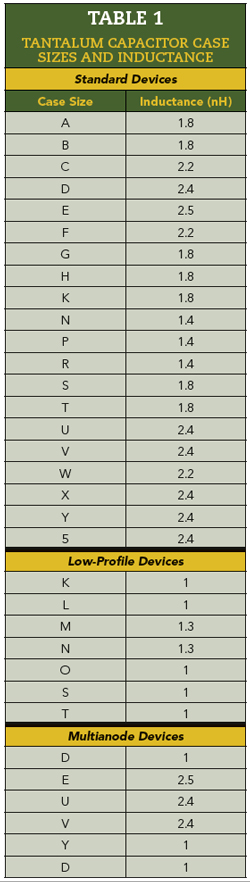
Tantalum and tantalum-polymer capacitors are available in multiple case sizes with reduced height profiles relative to aluminum electrolytic capacitors and with novel lead frame packages that have dramatically lower inductances than aluminum electrolytic capacitors (see Table 1 and Figure 5). This enables bulk capacitor designs with better fit. As such, both tantalum and tantalum-polymer capacitors are highly competitive with aluminum electrolytics and well suited for use in GaN power amplifier designs, despite their derating.