
UNIQUE CAPACITORS AND DC BLOCKING
Another passive component requirement for GaN power amplifiers is DC blocking. DC blocking in circuits operating at higher frequencies and wide bandwidths requires stable, low loss capacitors that can be easily configured to the circuit. Three unique capacitor technologies are worth considering: ultra-broadband capacitors (UBC), metal-insulator-metal (MIM) capacitors and metal oxide semiconductor (MOS) capacitors (see Figure 6). While there are additional options, these three types have proven to be practical for DC blocking.
UBCs — UBCs have a multilayered ceramic dielectric form factor that is compatible with standard printed circuit board manufacturing, including fully automated, high speed pick-and-place processing. They are available in 0201 and 0402 package sizes to match transmission lines, respectively, rated for 10 and 100 nF and they have ultra-low insertion loss, flat frequency response and excellent return loss from 16 kHz to approximately 70 GHz (see Figure 7). UBCs are an optimal passive component for DC blocking, DC coupling, bypass and feedback circuits in GaN power amplifiers.
MIM Capacitors — MIM capacitors are small, have low loss and can be used to compensate for the inductance effects of wire bond attachments, making them useful for DC blocking in high frequency transmit and receive stages. MIM capacitors use quartz, alumina or glass substrates to minimize loss and have a transmission line wire bond pad with backside ground to extend the frequency performance and reduce loss. Copper traces maximize conductivity, and front and backside gold metallization are compatible with high integrity epoxy, gold wire or ribbon attachment. They have 60 ppm/°C temperature stability with capacitance values from 0.3 to 15 pF and up to 100 V operating voltage. Custom capacitors can be designed, using a 50 to 100 pF/mm2 capacitance to area ratio.
MOS Capacitors — MOS capacitors are SLCs with SiO2 dielectrics and are small, temperature-stable capacitors with high Q, high breakdown voltage and low leakage. Manufactured with copper terminations in standard or custom patterns, MOS capacitors can be as thin as 127 μm for integration in 2.5D and 3D multi-chip modules, enabling higher frequency and lower power designs—potentially eliminating the wire bonds to the capacitor to reduce series inductance and extend the frequency response. Other termination options are gold or aluminum metallization on the top side and no metallization silicon, gold on bare silicon or chrome-gold on the bottom. Standard MOS capacitors are compatible with epoxy and solder die attachment and gold or aluminum wire bonding. Standard sizes and capacitance values range from 0.010 to 0.070 in.² and 1.0 to 1,000 pF, respectively.
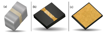
Figure 6 UBC (a), MIM (b) and MOS (c) capacitors.
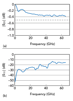
Figure 7 Typical |S21| (a) and |S11| (b) of the 550L series UBCs.
SMT HEAT PIPES
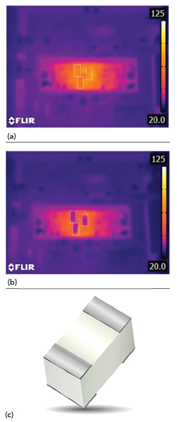
Figure 8 IR thermal scan of a 100-W GaN PA MMIC without heat pipes (a) compared to the PA using three heat pipes (b). Q-Bridge SMT heat pipe (c).
A signature benefit of GaN power devices is their ability to deliver high power in a small package. This can generate a massive amount of heat in a small area, requiring thermal control methods to remove, spread and couple the heat from the active device to get maximum performance and ensure reliability.
The thermal challenges of GaN can benefit from novel solutions like miniature SMT heat pipes.4 Miniature SMT heat pipes are a cost-effective solution for providing additional heat flow from the pins of an active device. Unlike traditional heat pipes, SMT heat pipes deliver high thermal conductivity with reduced parasitic capacitance, higher insulation resistance and high breakdown voltage. The small size of the SMT heat pipe supports the requirements for small size, weight and power (SWaP) designs. Although performance depends on the case size, the typical parasitic capacitance for the standard 0402, 0603 and 0805 EIA sizes is just 0.04 to 0.13 pF and the typical thermal conductivity is from 40 to greater than 500 mW/°C.
Miniature SMT heat pipes are available with several terminations: Sn/Ni/Pt, Ag/Pt and non-magnetic Ag. Custom SMT heat pipes have been designed to optimize the heat flow around MMICs, other high-power devices have been developed in case sizes spanning 0302 to 3737.
To illustrate the effectiveness of the SMT heat pipe, AVX engineers performed infrared (IR) measurements on an ultraminiature, high performance GaN power amplifier MMIC rated for 100 W output power. The MMIC was operated with a CW signal for 20 seconds at the amplifier’s center frequency, measuring the thermal rise with no heat pipes and using three Q-Bridge SMT heat pipes. Using the heat pipes, the IR measurement showed a 38°C decrease in MMIC temperature without any design modifications (see Figure 8), from approximately 80°C with no heat pipes to 42°C using the heat pipes. Neither the MMIC nor the larger power amplifier assembly were designed to include the Q-Bridge SMT heat pipes, i.e., the test was run with an existing design. Arguably, greater heat reduction could have been demonstrated if the power amplifier had been designed to include these SMT heat pipes.
SUMMARY
GaN RF power devices have been proven through extensive lab tests and products, hastening their deployment for defense and commercial applications, in turn driving prices down and increasing accessibility. To fully realize GaN’s impressive performance—reduced capacitance, higher electron mobility, low conduction losses, faster switching and higher frequency-temperature and frequency-voltage characteristics than silicon—engineers must pair GaN devices with high performance passive components. Passive components are important circuit elements for impedance matching, bias filtering, DC blocking and thermal management. Without paying attention to the effects of these passive components, designers risk limiting the technology from reaching the full capabilities of its performance.
The development of new material systems, such as the GBBL ceramic dielectrics for SLCs and conductive polymers for tantalum bulk capacitors, are enabling designers to mitigate these potential performance limitations. New capacitor sizes and package styles are enabling smaller layouts to support SWaP requirements and improve electrical performance. New devices like SMT heat pipes are expanding the solutions available for removing, spreading and coupling the heat from the higher power density of GaN—improving both performance and reliability.
As GaN device technology continues to evolve and deliver improved performance, new and improved passive component technologies will be engineered to support these impressively compact, low loss and fast switching semiconductors, leading to the next generation of smaller, lighter and more reliable RF power amplifiers.
References
- T. J. Green, “Microwave Packaging Technology.” TJ Green Associates, LLC Virtual Training Course, June 13–15, 2021, www.tjgreenllc.com/virtual-training/.
- Qorvo, “Application Note: GaN Bias Circuit Design Guidelines,” October 2019, www.qorvo.com/products/d/da006903.
- T. Zednicek, “High CV MLCC DC Bias and Ageing Capacitance Loss Explained,” European Passive Components Institute, November 2019, epci.eu/high-cv-mlcc-dc-bias-and-ageing-capacitance-loss-explained.
- R. Demcko, “The Impact of High Temperature Exposure on Capacitor Reliability and Performance,” AVX SEMI-THERM® Thermal Technologies Workshop, November 2020, semi-therm.org/wp-content/uploads/2020/11/TTW2020-Final-Program-DRAFT-20201103.pdf.