
Full duplex (FD) has the potential to double wireless communications capacity by simultaneously allowing transmission and reception (STAR) on the same frequency channel. In this article, a single antenna architecture with a hybrid coupler to isolate transmit and receive paths is evaluated. The fourth port of the hybrid coupler is terminated with a variable impedance (ZV), which is tuned for maximum self-interference cancellation (SIC) between the paths. ZV consists of a Wilkinson power splitter with its two splitting ports connected via a variable attenuator and variable phase shifter. This allows an incident signal applied at its summation port to be reflected back into the hybrid with an arbitrary gain and phase relative to the incident signal. Using a commercially available sleeve dipole antenna, up to 53 dB SIC is achieved over a 20 MHz bandwidth in the 2.45 GHz industrial, scientific and medical (ISM) band.
The pursuit for ever greater wireless connectivity has led to a rapid evolution of Wi-Fi standards over the last decade, each offering greater capacity in an already crowded spectrum. One proposed technique which can theoretically double data capacity is FD by allowing STAR on the same frequency.1-4 STAR, however, is limited by self-interference, where the transmitted signal interferes with the received signal. Transmit power can often be 100 dB greater than the power of the received signal. Not only does this degrade the signal-to-noise ratio of the received signal; it can also damage sensitive receiver circuity.
Some FD architectures use separate antennas decoupled by polarization2 and/or isolated by physical separation.3 However, the complex antenna design or extra space needed to accommodate two separate antennas often makes these approaches unfeasible. Single antenna solutions where the transmit and receive paths are coupled to the same antenna with a passive RF network are more practical. Most single antenna FD development has been based on circulators.4 Unfortunately, circulators are often too large and expensive for consumer electronics. Transmission line networks like the rat-race combiner,5 hybrid coupler1,6 and directional coupler7 are more practical. They also offer the possibility for greater integration, if the transmission lines are replaced with lumped elements.8
This work is based on a hybrid coupler, where the fourth port is terminated with a variable impedance, Zv. Zv is tuned to reflect part of the transmitted signal back into the coupler so it destructively interferes. When aligned in amplitude and phase, a high level of SIC is possible. Although the focus of this work is Wi-Fi communications in the ISM band, it can be applied to other applications, such as radio frequency identification,6 frequency-division duplex communications systems,9, 10 radar,5 test and measurement11 and backhaul.12
SINGLE ANTENNA FD CIRCUIT
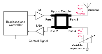
Figure 1 Single antenna, hybrid coupler full duplex system.
A simplified schematic of a single antenna, hybrid coupler FD system is shown in Figure 1. The baseband circuit generates an RF signal which is amplified by a power amplifier (PA) for transmission and applied to port 1 of a hybrid coupler with an equal (3 dB) power split. Port 2 of the hybrid is connected to a low noise amplifier in the receive path. In an ideal 50 Ω system, isolation between ports 1 and 2 exists due to the 180-degree phase difference between the two paths from port 1 to port 2. Half of the PA output signal is passed to the antenna at port 3 (VTRANS) and the other to the variable impedance ZV at port 4 (VIN). Part of VTRANS is reflected by the antenna due to mismatch, denoted as the vector VANT. The gain and phase of VANT relative to VTRANS is a factor of the antenna impedance and the length of cable connecting it to the hybrid coupler. Similarly, part of VIN is reflected by ZV and denoted as vector VZV. ZV is controlled by the baseband circuit, so that VZV and VANT cancel at port 2.
To provide a high degree of SIC, VZ must have the same magnitude as VANT and opposite phase. To do this, it must meet the following requirements:
(1)Sufficient range to cover the required band
(2)Sufficient resolution such that VZ = -VANT
(3)VZ must match VANT over the whole signal bandwidth.
The simplest published implementation of ZV consists of a single variable capacitor, which is tuned in only one dimension and, therefore, cannot simultaneously meet (1) and (2).1 Two-dimensional designs such as those based on vector modulators,13 can meet (1) and (2) but are often narrowband.14 Three dimensional multi-tap delay lines can meet all three requirements but are complex, making them unsuitable for consumer electronics.3,9
This article describes a new two-dimensional ZV consisting of a Wilkinson power splitter with its two output ports connected through a variable attenuator, A, and variable phase shifter, θ (see Figure 2). VIN enters the splitter and leaves it as two equal signals, V1 and V2. After passing around the loop through variable phase shifter θ and attenuator A, the signals are injected back into the hybrid coupler as VZV. A and θ control the gain and phase of VZV relative to VIN. Due to the reciprocal nature of the network, the signal travels in both directions around the loop, overcoming the inherent insertion loss of the split.
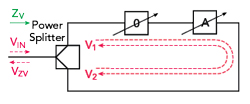
Figure 2 Two-dimensional variable impedance, ZV.
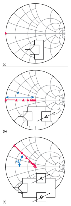
Figure 3 ZV operation: splitter with ports connected directly together (a), adding an attenuator to control the magnitude of VZV (b) and adding a phase shifter to control the phase of VZV (c).
The operation of the injection loop ZV is explained further in Figure 3. In Figure 3a, the two output ports of the splitter are connected directly together with a zero-length transmission line. Assuming a standard Wilkinson power splitter composed of two λ/4 sections, there is a 180-degree phase shift through this path. Looking directly at the input node, ZV appears as a short circuit. Adding A (see Figure 3b) allows the magnitude of VZV to be controlled, so that ZV can appear as a short circuit, 50 Ω at maximum A or any impedance between the two. Incorporating θ in the network allows the angle of VZV to be rotated around the Smith Chart (see Figure 3c).
The insertion loss of A and θ restricts the magnitude of the mismatch that can be synthesized, since VZV will always be smaller than VIN. Mismatches from the individual components, which interact with VZV, reduce the tuning range, as well. The most critical source of mismatch is from the input of the splitter, which tends to shift ZV away from the center of the Smith Chart, effectively introducing an impedance offset.14
SIMULATED SIC
To understand what level of performance - therefore SIC - can be achieved, the antenna mismatch must be characterized. Three commercially available sleeve dipole antennas, designated A, B and C, were measured (see Figure 4). They were measured in isolation, i.e., with no large metal structures nearby, but not in an anechoic chamber, so the data includes some environmental reflections. While all three have better than 10 dB return loss over the 2.4 to 2.5 GHz ISM band, antenna C performed the best. A return loss of 33 dB at 2.45 GHz indicates that VANT will have a magnitude 33 dB smaller than VTRANS. This means the antenna by itself provides 33 dB SIC if everything else is ideal. The role of ZV is, therefore, to provide greater SIC than the inherent 33 dB provided by antenna C.
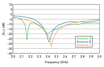
Figure 4 |S11| measurements on three dipole antennas.
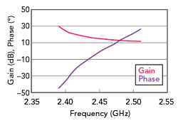
Figure 5 Simulated gain and phase settings for 60 dB SIC.
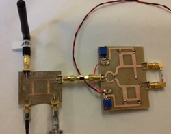
Figure 6 Prototype system, with the hybrid coupler and antenna (left) and ZV (right).
The FD system in Figure 1 with injection loop ZV was simulated in Cadence AWR’s Microwave Office, importing the S-parameters of antennas A through C as sub-circuits. In the simulation, better than 60 dB narrowband SIC was achieved over all regions in the ISM band by tuning A and θ. The values of A and θ are shown in Figure 5 for antenna C; the tuning range was 18 dB for A and 72 degrees for θ.
IMPLEMENTATION