
Applications continue to expand for mmWave and THz frequencies in aerospace, military, industrial and consumer markets. The result is increasing demand for faster and more reliable methods of testing waveguide components. At these frequencies, a rectangular waveguide is commonly used to carry the signals between components and subassemblies, with standard and non-standard flanges as the predominant means for connecting waveguide sections. When joined, precisely machined flanges provide continuous electrical contact around the mated waveguide openings.
Unfortunately, measurements of waveguide components are easily compromised by poor connections. Common problems include waveguide cocking, which occurs when flange surfaces are not perfectly parallel. Small gaps between the mating flanges can lead to power leakage and poor return loss, causing unreliable and inaccurate measurements.1,2 Repeated connections can also degrade the flanges used on waveguide test equipment such as vector network analyzers (VNAs), frequency extenders, power meter heads, frequency converters and calibration standards. Periodic replacement of expensive test system components is often required to maintain accuracy and repeatability.
Inadvertent gaps and surface damage may be minimized by carefully and evenly tightening the screws that provide mechanical contact between the waveguide flanges. However, this requires substantial training and skill to be performed correctly. When done repeatedly in a production environment, this work requires endurance and discipline. Ultimately, using traditional waveguide flanges in manufacturing operations limits how quickly and reliably components can be tested and sorted.
This article describes a contactless waveguide flange (CWF) that can be used without the flange screws mandatory with conventional flanges. When used with streamlined test fixtures, the CWF enables much faster mmWave and THz measurements while maintaining accuracy and reliability. The CWF was developed to preserve the electrical and mechanical integrity of both the device under test (DUT) and the test system, without sacrificing measurement results.
THEORY OF OPERATION
The CWF employs gap waveguide technology while applying the well-known principle of operation of the choke flange. The CWF choke is a recessed ring engraved into the flange at a nominal depth of λg/4 and a distance λg/4 from the waveguide walls, where λg is the guide wavelength. Gap waveguide technology has been thoroughly investigated and used previously in the design of antenna array feed structures and other passive components.3 These studies demonstrate that when a perfect magnetic conductor (PMC) plate and a perfect electric conductor (PEC) plate are positioned so they are parallel to each other and the distance between them is less than λ0/4, where λ0 is the wavelength of the operating frequency in air, a cutoff condition is created. As a result, parallel plate transmission modes cannot propagate between the plates.
Further, textured surfaces formed by metallic pins attached to a ground plane can exhibit the electrical characteristics of a PMC, forming an artificial magnetic conductor (AMC) over a limited range of frequencies. Often referred to as a “bed of nails substrate,” such an arrangement can be used to suppress dielectric surface waves in planar antenna structures. In the CWF, the choke ring is populated with concentric rings of small, pin-like structures to realize a high impedance AMC surface that approximates a PMC plate. Conversely, the mating surface on a conventional flange is flat, approximating a PEC plate.
The combination of a choke ring that controls the gap impedance and a band gap structure that suppresses signal leakage results in good signal transmission between the CWF and a conventional flange. In contrast to traditional flanges, no physical contact is required. Fast measurements can be performed without engaging the traditional waveguide connection screws that must be carefully tightened.
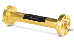
Figure 1 CWF implemented at E-Band.
The CWF concept has been demonstrated with an E-Band design (see Figure 1). It employs a standard waveguide flange modified by adding two concentric rows of pins to fill a choke ring engraved around the waveguide opening. The inner metal surface surrounding the waveguide opening has a nominal width of about λg/4 across the opening’s two longer sides. Its purpose is to transform an open circuit into a short circuit at the waveguide opening. Along the two shorter sides of the waveguide opening, the inner metal surface is thinner to increase the connection bandwidth.4,5
DESIGN CONSIDERATIONS
The first step in the design process is determining the dimensions of the pins to provide the stop band over the desired frequency range in the gap between the flanges.5 A unit element with periodic boundaries was used to calculate the stop band of the periodic electromagnetic (EM) band gap structure. The height of the pin surface is around λ0/4 at the center frequency of 75 GHz. The pin width and the distance between the pins affect the stop band of the combined AMC and PEC surfaces. However, the stop band is also affected by the pin height and the resulting thickness of the air gap between the AMC and PEC surfaces; the bandwidth increases as the gap between the two surfaces decreases. The stop band also moves lower in frequency as the height of the pins increases, following an inverse relationship.4
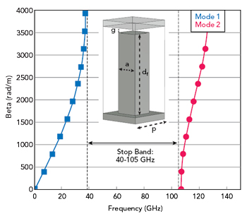
Figure 2 Dispersion diagram for an infinite periodic pin unit cell, showing the stop band from 40 to 105 GHz.
CST Studio EM simulation software was used to model the design (see Figure 2). The dispersion diagram shown in the figure applies to a unit element with an air gap (g) of 3 mils, pin height (df) of 35 mils, pin surface width (a) of 15 mils and pitch (p) of 25 mils. The stop band covers 40 to 105 GHz, covering all of E-Band (60 to 90 GHz).
Unlike previous designs, this design combines the functions of a choke flange with gap waveguide technology to suppress signal leakage and minimize reflections.6-11 The two rows of pins form a circular pattern to ease the mechanical design and fabrication of the pins. The pins form an AMC surface that creates a parallel plate cutoff condition at the junction between the waveguide flange surfaces, reducing signal loss and reflection. The present E-Band gap adapter design has a fixed air gap of 3 mils, although smaller gaps can be used to achieve better performance.
The CWF design was refined by performing repeated simulation and iteration. The process involves trade-offs between the electrical performance and manufacturability. In the present design, |S11| was evaluated for different gaps between the waveguide flanges (see Figure 3). From 60 to 90 GHz, the simulated return loss is better than -30 dB for a 3 mil gap and -40 dB for a 1 mil gap, indicating that good electrical performance is achievable without requiring any physical contact between the flanges.
The rim surrounding the waveguide opening has the same height as the pins. Its short walls are 14 mils thick, while its long walls are nominally 45 mils thick across the longer dimension of the waveguide opening. Another rim with radial thickness of 47 mils surrounds the pin array that forms the AMC surface. This external rim protects the pin surfaces from damage and determines the minimum gap between the AMC and PEC surfaces (see Figure 4). Guide pins are included to ensure proper alignment between the CWF and the conventional flange, adhering to standard flange definitions. By eliminating screws, measurements can be performed considerably faster, since the flanges only need to be aligned and pushed together.
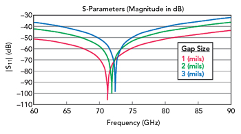
Figure 3 Simulated |S11| vs. gap size, showing effect of reflections at the waveguide flange interface.
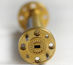
Figure 4 To prevent damage to the pin surfaces, the front face of the CWF has an outer rim 3 mils thicker than the pin array.