
A comb generator is a device with outputs that are multiple harmonics of an input signal. The output spectral tone lines are uniformly spaced at integer multiples of the input reference. A spectrum analyzer display of the output looks much like the teeth of a comb, which is how the device gets its name.
Comb generator devices fill many useful places in modern microwave systems. The most widely employed use is in broadband frequency synthesizers where high frequency signals provide stable system reference outputs correlated to lower frequency reference sources. The outputs may be delivered directly to other system components or fed to phase-locked loops as higher frequency references.
Microwave EW systems sometimes use comb generators to provide synchronous signals throughout large operating bandwidths for detection processing. Comb generators are even finding utility in consumer product testing markets where they are used to simulate radiated emissions for EMC testing.
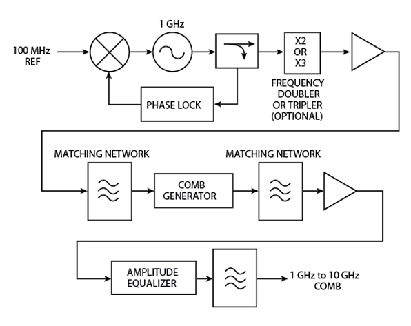
A line of comb generator multiplier products has been developed to meet this need. Models SYS0118A17N, SYS0218A17N and SYS0318A17N are broadband multipliers with 1, 2 and 3 GHz comb spacing. The model SYS0x18A17N contains a phase-locked oscillator with a 1 GHz output providing multiple benefits to the system designer. It allows for greater frequency separation of comb lines to reduce system filter demands. It also reduces the harmonic multiplication order for improved spectral efficiency without degradation of the output signal to noise ratio. Figure 1 shows a block diagram of the model SYS0x18A17N comb generator. Models SYS0218A17N and SYS0318A17N include a frequency doubler or tripler at the output of the phase-locked oscillator to properly control the frequency spacing at the output of the comb generator.
Step Recovery Diode Multiplier
The harmonic multiplier is based on MITEQ's standard multiplier product line technology. An input signal is amplified to a high level to excite a step recovery diode (SRD). The device characteristics of the diode cause a rich harmonic output of the 1, 2 or 3 GHz signal to be generated.
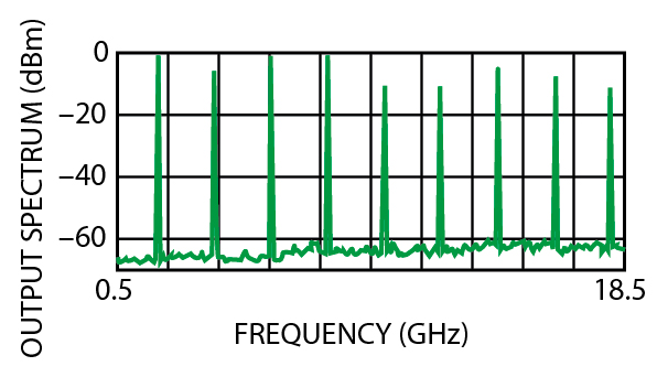
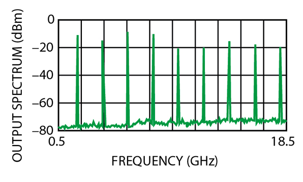
An SRD is chosen since the multiplications are orders of up to eighteen times the 1 GHz reference and can be performed with a single active stage. The SRD approach requires careful design to handle the wide instantaneous bandwidth, but offers the advantage of producing all of the required outputs as an immediately available composite signal without any subsequent spectral combinations. The higher power required to excite the SRD is generated with an efficient gain stage operating at a single frequency. Figure 2 shows the model SYS0218A17N comb generator's spectral output.
SRDs have low series resistance combined with a reactive impedance. Networks are inserted before and after the SRD circuit to improve impedance matching and increase power transmission efficiency. Preceding the SRD is essentially a low pass structure that simultaneously limits the bandwidth of the excitation amplifier output and provides an improved impedance match to the diode. A matching network with a high pass architecture is at the output of the multiplier. It is used for efficient power transmission of all of the comb tones to a broadband MESFET amplifier that follows the multiplier.
System Compatibility
The model SYS0x18A17N comb generator is designed to be compatible with many common microwave sources by accepting an input reference signal of 100 MHz. Current crystal technology supports generation of a 100 MHz signal which is highly stable over time, can be compensated well across wide temperature ranges and can exhibit very low noise spectrums.
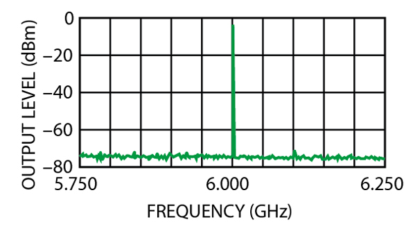
A common difficulty facing high order multiplier designers is that the spacing of the harmonically related tones potentially present a difficult filtering problem. Consider the case of a 100 MHz input directly multiplied to generate 2 GHz spaced tones from 2 to 6 GHz. At all output frequencies the tone spacing will be 100 MHz. Around 2 GHz there are strong signals present at 1900, 2000 and 2100 MHz. Both the upper and lower tones must be filtered to reject them to below the specified system spurious output requirement as these signals may feed through to the system output due to their proximity to the reference signal. Typically, this will mean a rejection of > 60 dBc at five percent from the desired reference of 2000 MHz.
Now consider in the example the case of the desired output at 6 GHz. Again there will be tones present at relatively high levels - 100 MHz above and below the desired output of 6000 MHz. A band pass filter with upper and lower skirts at > 60 dBc at only 1.7 percent from the desired reference will be required to maintain the system output spurious requirements. This rejection bandwidth is not trivial for even the most robust filter designs.
To overcome this limitation, the comb generator unit uses an internal phase-locked loop (PLL) with a VCO output of 1 GHz locked to the 100 MHz input. The tone spacing at the output of the multiplier is 1 GHz, 10 times that of a directly multiplied signal. This output spectrum places a system filtering demand of only 16.7 percent at 6 GHz, to a maximum of 5.5 percent bandwidth at an output as high as 18 GHz. Using model SYS0218A17N, which has tone spacing of 2 GHz, the filtering is achievable at an 11.1 percent bandwidth at 18 GHz. Figure 3 shows the resulting 100 MHz spurious output.
The use of a phase-locked loop to provide the initial multiple of 10 has additional benefits. The multiplication order required of the SRD circuit is significantly reduced. Using the output of the 3 GHz PLL, the demand placed on the SRD is to generate multiples of only six times the input, as opposed to multiples of up to 180 times the input if the reference signal were to be used directly. This technique eliminates the necessity of expending power to generate undesired intermediate tones, creating a more spectrally efficient output.
Phase Noise
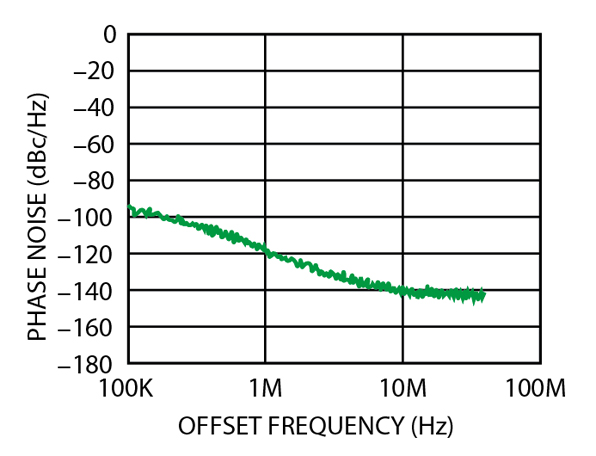
The phase noise performance of the device at offsets close to the output carriers experiences only minor degradation by employing a phase-locked loop for initial times 10 multiplication. The residual 1 GHz reference noise is then subjected to an increase of 20 log (N), where N is the multiplication factor. Inside the loop bandwidth this noise performance is minimally affected by the loop.
Outside the loop bandwidth the noise spectrum is governed primarily by the noise performance of the internal 1 GHz oscillator. Since the oscillator is internal to the device, the output phase noise performance will not vary with different reference input phase noise levels at frequency offsets greater than the loop bandwidth. Therefore, the output phase noise level at offsets greater than the phase-locked loop bandwidth can meet or be less than a direct 20 log (N) prediction of the input reference noise.
Phase noise of the 9 GHz output from the 3 GHz model was measured using the Aeroflex model PN9000 phase noise measurement equipment, using an oven-stabilized crystal oscillator as the 100 MHz reference input. The combined phase noise performance of the multiplier and the reference are lower than -140 dBc/Hz at a 10 MHz offset from the carrier, with a multiplication factor of 90, as shown in Figure 4 .
Amplitude Variation
A step recovery diode circuit generates outputs harmonically related to the 1 GHz internal reference, or to the doubled or tripled output. As the multiplication order increases, there is an increase in the amplitude variation of the individual comb lines. Reflections from the load the SRD sees looking forward into a broadband MESFET amplifier are likely an additional contributor to this variation.
Applications of comb generator devices typically have a need for minimally varying amplitudes of spectral components. To maintain a level output, a broadband matched amplitude equalization circuit is integrated into the design that maintains ±6 dB variation of model SYS0218A17N from 2 to 18 GHz. The higher the reference frequency used to excite the SRD, the less the variation in output comb amplitude.
Construction
Model SYS0x18A17N is constructed using a fully integrated architecture based on microstrip technology. The compact housing consists of machined walls to provide high isolation between circuit functions operating at different frequencies. Amplifiers carefully selected for noise, gain and bandwidth performance are integrated into the design to provide the necessary signal levels to each section of the system.

Environment
The comb generators are designed to operate in a variety of environments. Performance criteria of importance to systems are output reference leakage and output level stability. Measurements of model SYS0318A17N show no additional 100 MHz reference leakage when the case temperature is elevated to +70°C. The stability of the 2 GHz comb output of model SYS0218A17N was measured to be a variation of 3 dB from +25° to +70°C. The amplitude variation of the comb lines also remained within ±6 dB. The model SYS0318A17N comb generator's 100 MHz spurious output and the model SYS0218A17N comb generator's output spectrum are shown in Figures 5 and 6 , respectively.
Conclusion
A family of comb generator multipliers with high reference spurious rejections and level outputs in a fully integrated, compact and rugged device has been created. Options that are currently available are a switched filter output for individual tone selection, higher output power and lower overall phase noise. All of these optional configurations can be integrated into a single package to meet the demanding requirements of high performance microwave system architectures.
MITEQ Inc., Hauppauge, NY (631) 439-9423, www.miteq.com. Circle No. 300