Typical oscillator designs use a common-base or common-collector circuit for generating a negative resistance at one port, which is usually terminated with a parallel or series LC-resonant circuit. The main problems in this design are the bandwidth of the negative resistance, which cannot be easily extended over one frequency octave, and the low unloaded Q of commercially available SMD inductors, which leads to a decreased phase noise performance. However, there exist some advanced designs that cover more than one octave. Highly sophisticated oscillators, using YIG spheres or cavity resonators, are physically large and not easily tuned by electromechanical tuning or applied magnetic field. Dielectric- and ceramic resonator-based oscillators are small in size but poor in tuning range.

The basic idea of the design shown in Figure 1 is to use a varactor-tuned microstrip bandpass structure as feedback of an amplifier. This kind of oscillator design was proposed by Vidmar,1 who used a microstrip interdigital bandpass filter for frequency control. The differences between the two circuits will be discussed later.
Assuming that the amplifier has an infinite input and zero output impedance, the feedback loop can be broken up and the transfer function for steady-state conditions can be calculated in a straightforward manner.
If H(jω) is the transfer function of the amplifier and A(jω) is the transfer function of the filter, the loop transfer function G(jω) can be easily found by
(1)
G(jω) = H(jω) A(jω)The Barkhausen criterion for oscillation implies that the phaseshift in the loop must be zero and the gain equal to one. This means that
(2)
G(jω) = 1e j0° = 1
Therefore, the loop condition for oscillation is defined as
Replacing A(jω) with the characteristic transfer function of a second-order bandpass system2, the amplifier requirements become much clearer.
where
Q = quality-factor of the filter
A0 = amplification at the center frequency
Ω = normalized frequency variable
Oscillation should take place at the center frequency of the filter and so the condition Ω = 1 will be evaluated where
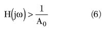
The factor A0 is usually somewhat lower than 1, which means loss in the filter network. Therefore, the amplifier must have some excess gain to generate the oscillation.
For the oscillation start-up, it is important that the amplifier has more gain than necessary as shown in Equation 5. The start-up requirement will be
In theory, the oscillation amplitude in the circuit would then rise to infinity, but because of the limitating properties of the amplifier, the level reaches a steady-state condition. The power supply voltage limits the amplitude of the oscillation. Through nonlinear effects in the semiconductor, the large signal gain is somewhat lower than the small signal gain. Both of these effects are sources of harmonics in the output signal of the oscillator.

Another problem in oscillator design is unwanted phase shifts through the active device and transmission lines between amplifier and resonator. To prevent the oscillation from quenching, the loop conditions in Equation 5 must be satisfied over the whole frequency band. Therefore, some extra phase shifting circuitry is necessary, as shown in Figure 2 .
Phase Shifters
The phase shifters are built as semi-lumped II low pass filters using varactors for phase tuning, while the inductor is realized as a microstrip transmission line. The basic idea is that low pass filters can have a nearly constant phase slope in the passband region. Through the variable capacitance of the varactors, the cut-off frequency of the filter can be moved, and therefore the phase slope can be adjusted. The assumption of a linear phase is approximately valid up to the cut-off frequency. In a first-order approximation, the phase slope of the phase shifter (group delay) is defined as
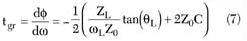
where
ZL = characteristic impedance of the transmission line
θL = electrical length of the line in degrees
ω L = frequency where θ L is defined
C = capacity of the varactor
Z0 = characteristic impedance of the system
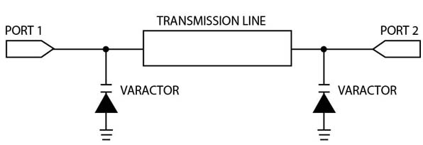
Figure 3 shows a schematic of the phase shifter.
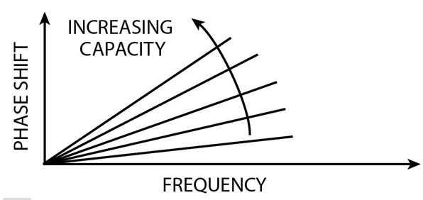
As can be seen in Figure 4 , the phase slope can be adjusted through the varactor tuning. The purpose of the phase shifter is to maintain a total phase shift of 360° in the loop, so that oscillations can occur. When designing the phase shifters, extra consideration must be given to the transistor phase shift. Through large signal effects, the phase shift in the transistor can be significantly different from that given by the small-signal S21 parameters. The parameters that influence the design of the circuit are
- Transistor phase shift at oscillation power-level
- Transmission line phase shifts
- Input- and output-impedance of the amplifier
- Input- and output-impedance of the bandpass filter
- Oscillation frequency
Bandpass filters are always designed for certain input- and output-impedances. The quality-factor of the filter is only valid at these defined termination resistances. The amplifier impedances should be as close as possible to these values, to maintain a high loaded Q and a low noise figure. A remaining mismatch between the amplifier and the bandpass filter can be resolved with the phase shifters. Another advantage of the proposed circuit is the low pass filter characteristic, which reduces unwanted harmonics at the output.
Combline Filter
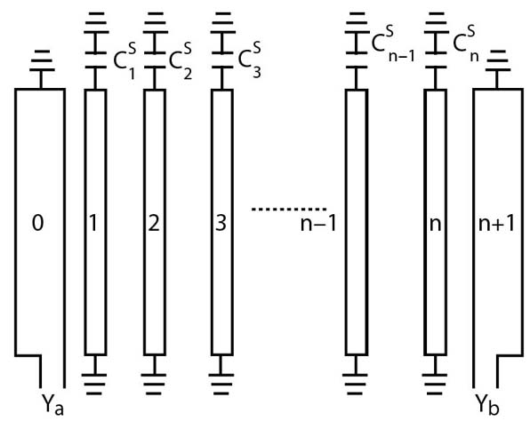
Figure 5 shows a combline bandpass filter in stripline form. The resonators in this type of filter consist of TEM-mode transmission line elements that are short-circuited at one end and have a lumped capacitance  between the other end of each resonator line element and ground. Lines 1 to n and their associated capacitances,
  to
to  , constitute the resonators, while lines 0 and n+1 are not resonators but simply part of the impedance-transforming sections at the ends of the filter. Coupling between the resonators is achieved in this type of filter by way of fringing fields between resonator lines. With the capacitors present, the resonator lines will be less than λ /4 long at resonance, and the coupling between resonators is predominantly magnetic. If the capacitors were not present, the resonator lines would be a full λ /4 long at resonance, and the structure would have no passband. For the reasons described above, it is usually desirable to make the capacitances in this type of filter sufficiently large that the resonator lines will be λ /8 long at the primary passband (the reentry passband would be four times the primary one).3
The advantages of this filter architecture are compact size and wide tuning range (in this case 600 to 2200 MHz). Adequate coupling can be maintained between resonator elements with sizeable spacings between resonator lines (this feature means that the proper couplings can be maintained in manufactured filters without unreasonable tolerance requirements).
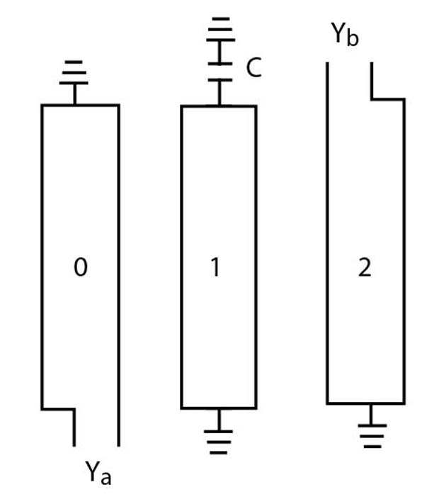
In the case of the oscillator, a filter with only one resonator is used, as shown in Figure 6 . However, filter configurations with two or three resonators have been tested as well, resulting in lower insertion loss at higher filter Q values.
Because the transistor amplifier uses a common emitter configuration, an approximately 180° phase shift is obtained. To keep the phase shifter small in size, the impedance node has been turned around to obtain an additional 180° of phase shift.
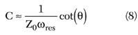
The capacitor C needed for a given resonance frequency is approximately defined as
because adjacent lines influence the effective resonator length
where
Z0 = characteristic impedance
θ = electrical length of the transmission line 1
This Equation describes simply the effect of compensating the inductive reactance of the short-circuited transmission line with a capacitor. The loaded Q of the filter is primary dependent on the width of the gap between the resonator and the impedance matching lines. The higher the gap width, the higher the quality factor. An exact calculation of the filter's quality factor is not easy, as the odd- and even-mode impedances of the coupled lines must be known. Since losses also increase with widening gap, the maximum Q available in the oscillator is limited by the amplifier gain, which should compensate for the filter losses. As opposed to the oscillator shown in Vidmar,1 where several varactors (up to nine) are needed to tune the phase velocity of an interdigital bandpass filter, in this case only one varactor can tune the oscillator frequency in a range of 1:3 or more. Additionally, the structure is very compact (more than 70 percent smaller) and is therefore low noise, small and less vulnerable to EMI.
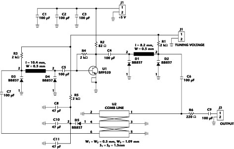
The detailed schematic of the oscillator can be seen in Appendix A . The transistor used is a BFP520 from Infineon that offers good RF data. A small-signal gain of 20 dB at 1.8 GHz and a transit frequency of more than 45 GHz with a low noise figure makes this transistor ideal for this oscillator circuit. For bias stabilization, a parallel voltage feedback circuit is used. The varactors BB857 are also from Infineon and can be tuned from 0.55 pF at 28 V to 6.5 pF at 1 V, with a low series resistance of approximately 2 Ω and a series inductance of 0.5 nH. R1, R3 and R5 provide the tuning voltage, and should have values that are neither too low, due to losses in the loop, nor too high, due to noise. Selected inductors without resonances in the operating frequency band could also be used. The output is coupled from the loop with a 220 Ω resistance, and should be followed by an amplifier because of the low oscillator level of approximately 0 dBm, and to avoid load pulling. The microstrip lines were printed on a 1 mm thick, low cost FR4 substrate with a dielectric constant of approximately 4.6. The supply voltage is a nominal 5 V and the circuit consumes about 40 mA. A good point to start with the combline filter design is to estimate the noise in the varactors through bias-resistances and self-noise effects, and calculate from that an appropriate filter Q value.
Performance
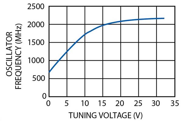
The tuning range was about 580 to 2200 MHz, as shown in Figure 7 . The power output of the oscillator was approximately -10 dBm at 600 MHz and +5 dBm at 2200 MHz. This is typical for the combline bandpass filter, as the coupling length compared to the wavelength shrinks with increasing frequency, and therefore less energy can be coupled in the resonator. This effect is partially compensated by the "decreasing with frequency" gain of the amplifier. However, the output power stays constant from approximately 900 MHz to 2200 MHz. Table 1 shows the power output after an MGA 81563 amplifier from Agilent has been connected to the oscillator. The harmonic content was a maximum of -20 dB for the second harmonic and -30 dB for the third over the whole frequency band.
The phase noise has been measured for several configurations that included (a) with single BB 857 varactors, (b) with back-to-back series MA4ST250-1141 high Q (Q ~ 400) varactors and (c) with fixed ceramic capacitors.
The phase noise performance was measured with an HP 8593E spectrum analyzer and the measured data has been used for a simple noise model using Leeson's noise equation,4 as very low power levels near the carrier could not be separated due to the spectrum analyzer's non-ideal IF filter frequency response. (~-90 dB pass through). The results are shown in Table 2 .
|
| ||||||||||||||||||||||||||||||||||||
 (10 kHz) (dBc)
Layout
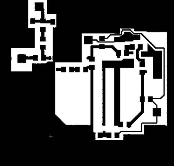
The oscillator circuit has been implemented on a simple 1 mm thick FR4 board with the dimensions 32 ´ 32 mm. Many vias are necessary to ensure good RF ground performance, especially at the combline filter line ends. Therefore, 2 to 4 holes with a diameter of 0.5 mm have been drilled for one ground path. All passive components have the standard 0603 size. The transistor comes in a SOT 343 and the varactors in a SCD-80 package. The layout of the oscillator with an MGA 81563 amplifier is shown in Figure 8 .
In the future, a combline filter could be realized as a ceramic component for further miniaturization, and better wideband and noise performance. It is also interesting to note that this type of oscillator is very tolerant to changes in microstrip length and resonator gaps, and also transistor type. It is even possible to control the loaded Q of the oscillator by only changing the spacings between resonator and impedance-transforming lines without altering the oscillator performance. One must only ensure that the amplifier delivers sufficient gain to compensate for the filter losses. Practically, that means that increasing the loaded Q will also increase the oscillator lowest oscillation frequency point, and therefore decrease the bandwidth of operation.
Conclusion
A new type of oscillator has been presented. Through the special resonator construction, a compact size and low noise with wideband operation are possible. Low cost and high manufacturing tolerance susceptibility makes this circuit attractive for high volume applications.
Acknowledgment
The author wishes to thank Andrei Grebennikov for his technical suggestions, and Graz University of Technology for providing the measurement equipment.
References
1. M. Vidmar, "A Wideband, Varactor-tuned Microstrip VCO," Microwave Journal , Vol. 42, No. 6, June 1999, pp. 80-86.
2. U. Tietze and C. Schenk, Halbleiter Schaltungstechnik 10 , Auflage Springer Verlag., 1993.
3. L. Young, Microwave Filters Using Parallel Coupled Lines , Artech House Inc., Norwood, MA 1972.
4. D.B. Leeson, "A Simple Model of Feedback Oscillator Noise Spectrum," Proceedings of the IEEE , February 1966.
Gerhard A. Hofbauer received his Dipl. Ing. and MSc degrees from Graz University of Technology in May, 2002, and is now working toward his PhD degree at the same university. He can be reached via e-mail at gerhard@radar.TUGraz.at.
|
Appendix A |