
The ever-growing demand for data speeds and small form factors in modern electronic devices is driving an increasing demand for flexible circuits. Rigid-flex printed circuit boards (PCB) - a hybrid of hardboard and flexible circuits, where some layers are flexible circuitry running all the way through the hardboards (see Figure 1) - are used in many modern electronic devices because of their form factor, light weight and cost-effectiveness. They are preferred for mobile communications products because of their conformality, ability to fit into small spaces and low manufacturing cost.
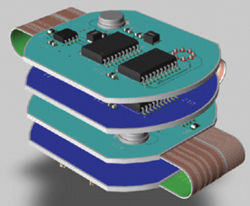
Figure 1 Rigid-flex PCB.
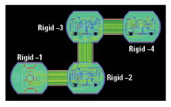
Figure 2 Rigid-flex PCB with four rigid and three flex zones.
Electromagnetic (EM) analysis of rigid-flex PCBs has always been challenging, namely modeling the complexity of bending a board into small spaces. A workflow using the Cadence®Clarity™3D Solver provides tool interoperability to enable designers to accurately verify the signal integrity of the rigid-flex traces using 3D finite-element method (FEM) analysis. Compared to traditional, more manual design processes, this flow is efficient to set up for EM simulation and, thus, less prone to human error.
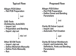
Figure 3 Traditional MCAD workflow (left) vs. automated Cadence Allegro/Clarity process (right).
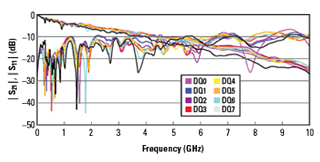
Figure 4 Simulated |S21| and |S11| for selected nets.
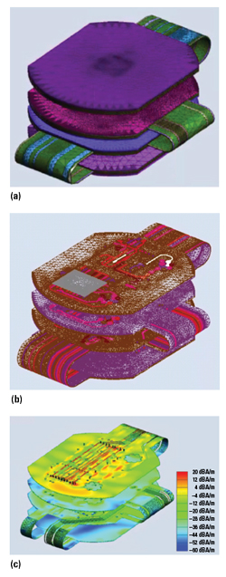
Figure 5 Mesh plots of the dielectric (a) and metal layers (b). Metal layer surface current density with all ports excited (c).
Cadence Allegro®PCB Editor is commonly used for designing rigid-flex PCBs, as it enables designers to easily create and visualize boards in real time. Features include rigid-flex transformation (i.e., bending), multiple flex laminates supporting flex circuit cover-lays, zone management for rigid and flex and checking coverage and clearances (i.e., interlayer checks). Once the board layout (ECAD) is completed by the PCB designer using the guidelines to fit the components in the required space, the ECAD data is imported into the Clarity 3D Solver, a full-wave 3D FEM EM simulator. The Clarity 3D Solver, used for designing critical interconnects for PCBs, IC packages and system-on-IC (SoIC) designs, leverages Cadence’s distributed multiprocessing technology to provide virtually unlimited capacity and 10x speed improvements for large-scale designs.
Compared to the workflow for simulating “flat” PCB geometries, the workflow for rigid-flex PCBs have additional complexity from combining the rigid board with a 3D flex board that can be bent and twisted in any direction (see Figure 2). The traditional approach for a rigid-flex board is a mechanical computer-aided design (MCAD) flow, where the board is first imported into a 3D MCAD tool like AutoCAD to perform the 3D bending. The bent board is then exported as a .step/.iges/.sat file and imported into a 3D EM tool for S-parameter extraction. This process is prone to human error during the bending process - via and layer misalignment and length mismatch - as well as within the EM tool, where material properties are defined and ports created. Even if the entire process is carefully carried out without error, the EM simulation may not run due to design complexity and meshing issues. Once this happens, the designer is in a loop between the MCAD tool, to clean the geometry, and the EM engine, to set up the simulation. This iterative effort requires significant user interaction and is time consuming, taking hours to days - even weeks in some cases - depending upon the scope of the design.
AUTOMATED WORKFLOW
The Cadence workflow addresses the challenge of rigid-flex bending analysis with a completely automated, easy-to-use solution that takes only a few minutes to set up with minimum input from the designer. The workflow is a five-step process:
1. Define the parameters in Allegro PCB Editor software
2. Import the parameters into the Clarity 3D Solver environment and verify the layer stackup, nets, components and different zones are correct
3. Define the ports using the automatic port wizard
4. Transfer the resulting .spd file into the Clarity 3D Solver’s workbench environment.
5. Define the solution frequency and frequency sweeps and run the simulation
These steps are illustrated in Figure 3, compared to the traditional, manual MCAD workflow.
To illustrate the automated workflow, a three-bend rigid-flex PCB simulation was performed using the Clarity 3D Solver at 10 GHz with a frequency sweep from 10 MHz to 10 GHz. The Clarity 3D Solver’s automatic adaptive finite-element mesh refinement provides consistent accuracy for the rigid-flex PCB. The parallelization technology ensures both meshing and frequency sweeping can be partitioned and parallelized across multiple computers, reducing the time to solve the entire, complex rigid-flex structure. The |S21| and |S11| for select nets of the rigid-flex board are shown in Figure 4. The mesh plots and surface current density on the metal layers are plotted in Figure 5, showing how bending the flex PCB is modeled.
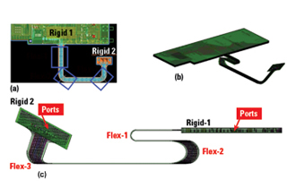
Figure 6 Three-bend rigid-flex board showing layout in Allegro PCB Editor (a), 3D view (b) and cross section in the Clarity 3D Solver workbench (c).

Figure 7 Mesh plot of the metal layers, with views of the flex circuit and rigid board.
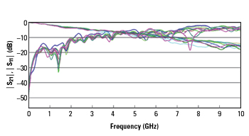
Figure 8 Simulated |S21| and |S11| for selected nets.
A second example illustrates a different type of three-bend rigid-flex board, one with three flex zones and two rigid zones (see Figure 6). The signal lines start at Rigid 1, run through Flex 1, Flex 2 and Flex 3 to end on Rigid 2. The ground plane consists of a diagonal: both cross-hatch (Xhatch) planes with a line width of 0.3 mm and spacing of 0.3 mm. The ports are defined on the two rigid sections shown in Figure 6(c). The circuit performance was simulated at 10 GHz with a frequency sweep of 10 MHz to 10 GHz. The mesh plots shown in Figure 7 indicate the level of modeling and analysis detail for the Xhatch ground planes, bending regions and signal nets using the Clarity 3D Solver. Figure 8 plots the simulated |S21| and |S11|, showing the slight variations in the frequency response as a function of the bending parameters.
CONCLUSION
The rigid-flex PCB workflow is one example of how an integrated design and EM analysis solution can accelerate product design cycles. This simple and efficient workflow for the EM analysis of rigid-flex PCBs saves both PCB and EM designers time setting up and analyzing the design. This workflow using the Clarity 3D Solver can be used by EM engineers to streamline design steps and achieve quick time-to-market product development.
For more information about the Clarity 3D solver, click here.