
With multiple software defined radio (SDR) transceiver IC and a new high performance multi-processor system-on-chip (MPSoC), an SDR-based wideband MIMO transceiver prototype delivers high amplitude and phase consistency and parallel processing of complex wideband MIMO signal processing algorithms. It transmits and receives multi-channel signals with bandwidths up to 200 MHz over a tuning range from 75 MHz to 6 GHz.
In recent years, there has been tremendous theoretical research on massive MIMO (mMIMO) systems in areas such as capacity analysis, channel estimation, synchronization, beamforming techniques, user scheduling and spectral efficiency.1 Communication and radar systems employing MIMO techniques require higher and higher bandwidths with stringent requirements on in-band flatness and amplitude-phase consistency across multiple channels. Small size and low cost are also desired. Thus, small, highly integrated, SDR-based MIMO transceivers have recently been proposed.2-4
Traditional multi-channel data acquisition systems have low channel integration and limited transmission rates, which cannot meet today’s needs for miniaturization, high bandwidth and deterministic delay.5 Deficiencies exist both in bandwidth and the signal processing capability of conventional SDR-based MIMO transceivers. For example, the agile AD9361 SDR transceiver has a maximum bandwidth of 50 MHz.5-7 It cannot meet the requirements of evolving MIMO communication and radar systems, which often require instantaneous bandwidths of hundreds of MHz to over 1 GHz. With increased signal bandwidth, higher sampling rates are needed, resulting in a significant increase in signal processing payload. This drives the need for higher performance computing systems, programmable devices with parallel processing ability and even heterogeneous devices with multiple types of processing units.
Development of commercial off-the-shelf (COTS) SDR transceiver ICs and signal processors make it possible to address such deficiencies. For example, Analog Devices’ ADRV9009 is a highly integrated, two channel, agile transceiver. It supports receiver bandwidths to 200 MHz, transmitter bandwidths to 450 MHz, and has a tuning range from 75 MHz to 6 GHz that can satisfy the bandwidth and center frequency requirements of 3G, 4G and 5G communication systems. The analog-to-digital converter (ADC) interface, using the high speed serial protocol JESD204B, can easily synchronize multiple channels. It does not require many I/O ports, reducing the complexity of layout and routing.8-11
Regarding signal processors, Xilinx has developed heterogeneous SoCs with multiple processor cores, including the Zynq-7000 series, the Zynq UltraScale™ series and the Zynq UltraScale+ series. The Zynq UltraScale+ series MPSoCs provides multiple, extensible, 64-bit central processing units, real-time control and a software/hardware processing engine capable of image processing, wave processing, complex MIMO communication and radar signal processing. The EG devices of the Zynq UltraScale+ series MPSoCs carry both a processing system composed of Quad ARM Cortex-A53 cores running up to 1.5 GHz and the Xilinx programmable logic UltraScale+ architecture. The heterogeneous architecture, on-chip memory, multiport external memory interfaces and a rich set of peripheral connectivity interfaces are suitable for wideband MIMO signal processing.
With multiple SDR transceiver ICs and the newest high performance heterogeneous MPSoCs, the SDR-based wideband MIMO transceiver prototype described in this work features high amplitude-phase consistency, a multi-channel transmit bandwidth up to 450 MHz and a multi-channel receive bandwidth up to 200 MHz, with a tuning range of 75 MHz to 6 GHz.
DESIGN
Architecture
The SDR-based wideband MIMO transceiver comprises a signal processing element (SPE), MIMO RF channels (MIMORF), a clock and synchronization element (CSE), a calibration element (CE) and a power element (see Figure 1).
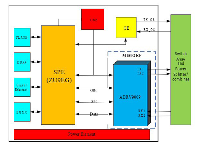
Figure 1 MIMO transceiver architecture.
The core SPE component is the heterogeneous Zynq UltraScale+ MPSoC. With its rich peripheral interfaces and connectivity, it provides the SPE with a heterogeneous parallel processing capability, high throughput memory, high throughput interconnection to RF transceivers and external devices and the extra connections required for multi-channel synchronization and calibration.
MIMORF comprises multiple, agile, SDR-based ADRV9009 transceiver ICs. With JESD204B data path interfacing, the serial interfaces save SPE pin connections, so even 16 channels can be connected to just one MPSoC of the SPE. This simplifies the design of multi-channel synchronization and calibration.
The CSE provides the system clocks, while also providing the synchronization signals required for the JESD204B interface and for multi-channel synchronization.
The CE includes circuits to provide multi-channel amplitude-phase consistency and calibration. There are two kinds of calibration schemes: the first is inboard calibration, which provides signaling and signal switches for calibration inside the MIMO transceiver; the second is system calibration, which uses signaling and signal switches outside the MIMO transceiver module. At times, calibration of the entire signal chain involves filters, RF cables and antennas. For complex signaling and signal integrity for wideband signals, CE chooses the second type of calibration scheme.
SPE Design
The Zynq UltraScale+ MPSoC connects to eight ADRV9009s via the JESD204B interface, to implement the 16-channel MIMO transceiver. Each ADRV9009 is connected by two-lane GTH serial lines (see Figure 2).
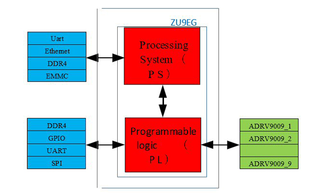
Figure 2 SPE design.
The Zynq UltraScale+ MPSoC consists of two computing units, PS and PL, connected by the on-chip AXI interface. PS is a multi-processor unit implementing DMA transmission, AD9528 configuration, ADRV9009 configuration and channel calibration, while PL is programmable logic implementing the JESD204B interface module, DMA controller and drivers for other peripherals like DDR4 chips.
Transceiver workflow and multi-channel calibration are conducted by PS and PL. PS receives commands and reports status via the Gigabit Ethernet. PS distributes tasks and accomplishes the multi-channel calibration algorithm. PL generates the test signal for calibration, acquires the data used for calibration and logically controls the test signal correctly looping back.
DMA transmission between PS and PL has a data width of 128 bits with a 300 MHz clock frequency; thus, the transmission data rate is 300 MHz x 128 bits or 38.4 Gbps. With a sampling rate of 245.76 MSPS, the data acquisition rate is 16 x 32 bits x 245.76 MSPS, which equals 25.83 Gbps, for there are 16 channels and every I/Q sample has a width of 32 bits. Because the acquisition data rate exceeds the DMA data rate, it is not possible to accomplish real-time transmission via DMA. Thus, the sampled signal is processed real-time in the PL. DDR4 is used to buffer the acquired data and the temporary variables in the PL. The 32-bit data width DDR4 double samples on the 1 GHz frequency, which achieves a raw throughput of 1 GHz x 2 x 32 bits, or 64 Gbps. There are four-lane GTH serial lines in a GTH bank in the PL. Two, two-lane ports are used to connect two ADRV9009s.
MIMORF and CSE Design
MIMORF comprises nine ADRV9009s, and the CSE is mainly the AD9528 clock chip. ADRV9009s use the JESD204B interface, which simplifies the layout of the ADC’s interface using serial ports. The AD9528 is a two-stage phased-locked loop, with multiple JESD204B SYSREF generators used to produce the clocks and synchronization signals needed by multiple independent channels.
Workflow of the multi-channel synchronization can be summarized as follows:
- Nine synchronized reference clocks are generated to feed nine ADRV9009s for clock phase synchronization of multiple channels.
- After issuing the configuration of all the ADRV9009s, JESD204B receivers in the MPSoC and in the ADRV9009s detect the K-code sent by JESD204B transmitters for link initialization. With K-code detected in every connected channel, the SPE MPSoC triggers the AD9528 to generate 10 SYSREF signals, nine of which are respectively connected to the nine ADRV9009s, while the remaining one is connected to the MPSoC. The SYSREF signal fed by the AD9528 to the PL in the MPSoC is fanned out to all JESD204B transceivers in the PL, used to connect to all nine ADRV9009s. With the synchronized SYSREF signals, MFCLK for different JESD204B transceivers between SPE and ADRV9009s are generated synchronously, which leads to synchronous transmission along the multiple channels.
- There is a synchronization scheme designed in the ADRV9009. The initial phases of the RF local oscillators and the baseband clocks are synchronized according to the synchronous SYSREF and the reference clock.
All the related clocks and data lines are routed to meet signal integrity requirements.
CE Design
The CE (see Figure 3) is designed to detect amplitude-phase consistency mismatch.
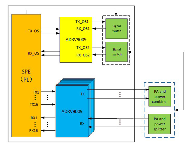
Figure 3 CE design.
One of the nine ADRV9009s is used for amplitude-phase consistency mismatch detection. Only one of the two channels is used, and a digital switch enables the use of just one RF port. With an external power splitter, the reference signal is distributed to the 16 channels. All captured data in PL is transferred to PS via DMA transmission for multi-channel consistency/mismatch detection calculation. An external signal combiner uses a time division scheme for amplitude-phase consistency/mismatch detection. The sinusoidal reference signal is distributed to multiple channels equally spread in time, channel by channel (see Figure 4).
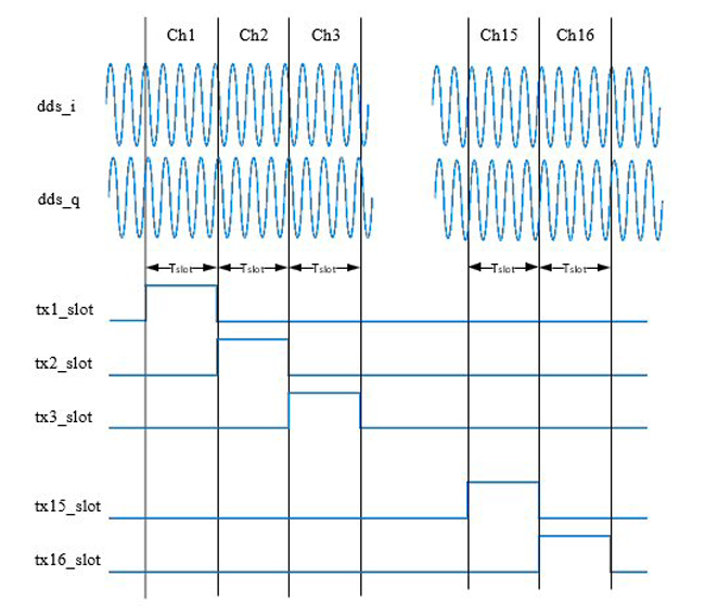
Figure 4 Transmit calibration timing diagram.
The sinusoidal wave can be generated by a direct digital synthesizer (DDS). As shown in Figure 4, if the time interval used by any channel is Tslot, then the signals captured can be written as:
where ∅0 is the initial phase of the DDS, while An is the amplitude and the phase added by the corresponding channel n. Tslot is the time slot interval, a fixed delay, while Δt is the time delay error caused by the transmitting channel feature and layout. Here ƒ0 is the frequency of the DDS.
A fast Fourier transform (FFT) is used to calculate the phase term in Equations (1) and (2). The amplitude consistency mismatch is determined by the amplitude multiplication operation. Before phase subtraction is executed to calculate multi-channel phase consistency mismatch, the extra phase term 2πƒ0Tslot (n-1) introduced by the time interval Tslot (n-1) should be canceled.
Although direct subtraction is a proper choice when Tslot is a known parameter, a better method is to use a predefined time interval, which leads to 2πƒ0Tslot (n-1) = m x 2π , where m is an integer.
The receiver’s amplitude-phase consistency mismatch is detected by simultaneously capturing the reference signal split to the 16 channels. After the captured data is transferred to PS, a similar procedure of performing an FFT, then the amplitude and phase subtraction, is carried out.
IMPLEMENTATION
The prototype (see Figure 5) uses the XCZU9E as the SPE core processor. Eight ADRV9009s implement the 16 transceiver channels, while an extra ADRV9009 is used for calibration. The prototype is a 6U board compliant with VITA 46.0 VPX standards.
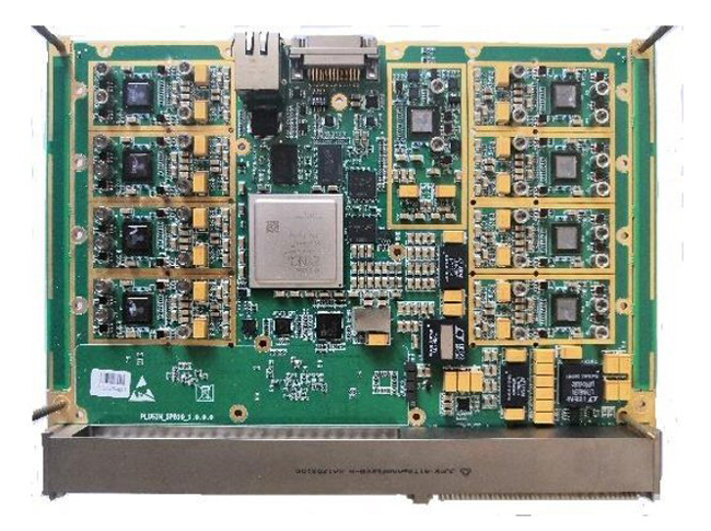
Figure 5 Prototype MIMO transceiver.