
As with all PA designs, the even-mode stability must be ensured across frequency and temperature, and the odd-mode stability of the combined auxiliary branch transistors must be considered. This is important when combining multiple transistors to increase gate width, which is the case with the auxiliary branch. Due to their class C bias, the auxiliary transistors do not provide small-signal gain, so odd-mode stability is ensured. Under large-signal operation, oscillations may occur, so stability simulations were run to determine the appropriate odd-mode stability resistors.
ON-WAFER MEASUREMENTS
The PA was measured using direct on-wafer RF probes in PRFI’s cleanroom, testing both small- and large-signal performance. Because the auxiliary branch is biased to operate in class C, Doherty amplifiers often have low small-signal gain. So the measured gain of 20 dB at 27 GHz and 18.6 dB at 30 GHz is notable (see Figure 3). Compared to the simulated performance, the measured small-signal gain is slightly higher, while the frequency response matches well with the simulations, reflecting the accuracy of both the Wolfspeed PDK models and the EM simulations of the on-chip matching networks.
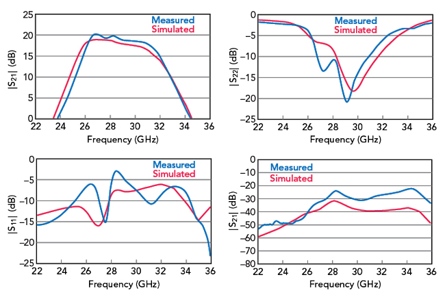
Figure 3 Doherty PA simulated vs. on-wafer measured S-parameters.
The maximum output power of the Doherty PA was 35 dBm (3.2 W). Because of the cable and probe losses, the driver amplifier could not fully compress the Doherty PA, so the maximum output power is expected to be higher when the packaged PA is measured. To manage the thermal dissipation of the PA, the large-signal measurements used a 100 μs pulse width, 10 percent duty cycle RF input. The efficiency of the PA at 8 dB back-off, 27 dBm (0.5 W) output, was 19 percent. This efficiency will likely be higher when the die is packaged and mounted on an evaluation board (EVB) with a better thermal environment. “Tuning” the PA bias may yield further improvement in power and efficiency.
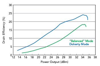
Figure 4 Measured on-wafer drain efficiency at 29 GHz.
Figure 4 shows the efficiency advantage of the Doherty configuration compared to a conventional class AB PA design. The “balanced” mode was measured by setting the same gate voltages for the auxiliary and main branch PAs. At an output power of 27 dBm (0.5 W), equivalent to 8 dB back-off, the measured Doherty efficiency is 19 percent, compared to less than 10 percent for the balanced case.
Compared to other published Doherty PAs at mmWave frequencies, this asymmetric GaN design achieved higher output power than GaAs versions and wider bandwidth than other GaN Doherty PAs, whether GaN on Si or GaN on SiC.5,6
PACKAGING
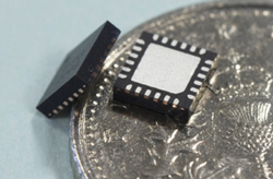
Figure 5 Doherty PA packaged in a 4 mm x 4 mm QFN.
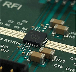
Figure 6 Packaged Doherty PA assembled on an evaluation board.
Packaging is a key aspect of PA design, especially at mmWave frequencies.7 For this design, a cost-effective plastic overmolded 4 mm x 4 mm QFN package was selected to give adequate protection to the die while being compatible with volume production (see Figure 5). For optimum performance and reliability, the thermal resistance between the transistor channel and the backside of the package should be minimized. While the MMIC substrate is SiC, which has excellent thermal properties, the thermal resistance between the backside of the die and the package die attach paddle (DAP) must be minimized. Typically, the die is attached to the DAP with an epoxy; using a high thermal conductivity epoxy reduces the junction-to-case thermal resistance. In addition to the bulk thermal conductivity of the epoxy, bond-line thickness, curing conditions and shear strength are also important considerations when selecting the epoxy.
The plastic overmold of the package is expected to shift the frequency response of the PA down. The die was designed for this, reflecting a higher frequency band when measured on-wafer so the packaged PA will be centered around the 26.5 to 29.5 GHz design band. The design includes guard bands above and below to accommodate MMIC and assembly process variations. The packaged PA will be extensively tested on an EVB (see Figure 6) and the measured data compared with die performance. The EVB uses minimal off-chip decoupling components and requires no off-chip RF components, as all RF components are integrated on the MMIC.
CONCLUSION
Combining PRFI’s experience designing mmWave MMICs and sub-6 GHz Doherty PAs with Wolfspeed’s G28v5 process, PRFI designed a Doherty PA MMIC suitable for the 28 GHz 5G band. An asymmetric topology demonstrated excellent initial results on the first-pass die design, with on-wafer measurements of at least 35 dBm output power, 27 dBm at 8 dB back-off with 19 percent PAE and 20 dB small-signal gain. The packaged MMIC will next be evaluated on an EVB to compare packaged and die performance. With wide bandwidth and flat gain, the MMIC PA assembled in a low cost 4 mm x 4mm QFN package will be useful for transmitters in 5G mmWave infrastructure systems.
References
- R. Smith, S. Glynn, J. Greene and L. Devlin, “A Fully Integrated 3.5 GHz Single Chip GaN Doherty PA for sub-6 GHz 5G,” ARMMS, 2019, https://www.prfi.com/wp-content/uploads/2019/04/ARMMS_3p5_GHz_Doherty_MMIC_v5.pdf.
- S. Glynn, G. Pearson, A. Dearn and L. Devlin, “The Design of a Plastic-Packaged PA for 28-GHz 5G,” Microwaves & RF, 2019, https://www.mwrf.com/technologies/semiconductors/article/21849808/the-design-of-a-plasticpackaged-pa-for-28ghz-5g.
- S. Glynn, R. Smith, L. Devlin, A. Dearn and G. Pearson, “Design of a Single Chip Front-End Module for 28 GHz 5G,” Microwave Journal, April 2018, pp. 22–34, www.microwavejournal.com/articles/30052-design-of-a-single-chip-front-end-module-for-28-ghz-5g.
- Wolfspeed, “GaN Foundry Services,” www.wolfspeed.com/rf/foundry-services.
- R. Giofre, A. D. Gaudio and E. Limiti, “A 28 GHz MMIC Doherty Power Amplifier in GaN on Si Technology for 5G Applications,” International Microwave Symposium, 2019.
- K. Nakatani, Y. Yamaguchi, Y. Komatsuzaki, S. Sakata, S. Shinjo and K. Yamanaka, “A Ka-Band High Efficiency Doherty Power Amplifier MMIC using GaN-HEMT for 5G Application,” IEEE Microwave Theory and Techniques International Microwave Symposium, 2018.
- L. Devlin, “Packaging for mmWave Devices - Why Do We Need It, and How Do We Do It?, ”RF Globalnet, 2019, www.rfglobalnet.com/doc/packaging-for-mmwave-devices-why-do-we-need-it-and-how-do-we-do-it-0001.