

The 5G market is undergoing a rapid transformation as networks and commercial services are deployed. mmWave spectrum will be indispensable, given the large swaths of contiguous bandwidth to support high capacity, with low latency and dense spatial re-use. Trials have culminated in the first commercial offerings, and regulatory agencies are adding even more spectrum from 24 to above 40 GHz.
Active antenna arrays and beamforming underpin the mmWave 5G architecture, enabling spatial re-use and helping overcome the high path loss at mmWave frequencies. This technology provides flexibility with the system design, to address urban and suburban use cases such as small cells, fixed wireless access and macro base stations, each requiring different equivalent isotropically radiated power (EIRP), mobility, interference tolerance and beam steering range. One common aspect for all use cases is that active antenna arrays require many antenna elements, from 16 to 1024 elements depending on the deployment scenario. They can be split into vertical and horizontal polarizations to transmit different sets of data to different users or to improve the link margin when serving a single user. Integrating more channels into a beamforming system is necessary to reduce the cost, power and board area of these systems, particularly as volumes grow.
As with each generational shift in mobile networks, operators are demanding the optimal cost/performance trade-off. In this environment, semiconductor suppliers capable of offering a cost-effective, end-to-end solution will play a crucial role in commercial, high volume 5G deployment and achieving the implementation cost, board area, system power and time-to-market goals. A complete system offering eases system-level optimization and calibration, freeing equipment manufacturers to focus on system performance, rather than having to optimize a multi-vendor lineup at the component level. A complete solution simplifies the radio manufacturer’s supply chain.
For hybrid beamforming architectures, as shown in Figure 1, Analog Devices’ “bits to beams” mmWave lineup provides a system-level offering encompassing the entire chain of digital, mixed-signal, IF and mmWave functionality - ending at the antenna array. Covering 24 to 30 GHz, ADI’s chipset comprises a 16-channel dual/single polarization beamformer IC (ADMV4821), 16-channel single polarization beamformer IC (ADMV4801), mmWave up-/down-converter (ADMV1017) and the MxFE™ RF data converter platform (AD9081 and AD9082). This chipset offers the highest integration, supporting the n257, n258 and n261 bands with a single footprint for each function.

Figure 1 Hybrid beamforming signal chain.
For maximum flexibility in the field, where dynamic adjustment to beam shape is critical, the beamformers feature a fast switching mode and beam storage. The MxFE, up-/down-converter and beamformer chipset is 3GPP compliant, providing best-in-class EIRP and error vector magnitude, tested using 5G New Radio (NR) waveforms with 64- to 256-QAM modulation. The closely coupled designs of the up-/down-converter and beamformers enable array calibration to optimize the beam profile to meet stringent use cases in the field. The dual-polarization beamformers address an emerging customer requirement for a single small, power efficient and low-cost active antenna system, rather than using two, single polarization arrays.
The up-/down-converter provides a range of IF options, i.e., either zero IF or one between 3 and 10 GHz. The MxFE data converters have high dynamic range and instantaneous channel bandwidths to 1.2 GHz to support multi-band architectures. Time-division duplex duty cycle modes enable the sharing of the receive path between traffic data and antenna array calibration steps, while maintaining phase coherency. Multi-chip synchronization ensures data timing alignment across multiple antenna arrays.
Integrating 16 channels simplifies the complexity of the mmWave radio design, leaving room for other components on the back of the antenna array. It reduces chip-to-chip variation for a given array size, reducing the component count from 2 to 4x compared to four or eight channel RFICs. As ADI demonstrated at the 2019 International Microwave Symposium (IMS), random amplitude variations up to ±1 dB and random phase variations up to ±10 degrees do not appreciably degrade the sidelobe level or beam gain at boresight and, therefore, the array does not need calibration (see Figures 2 and 3).
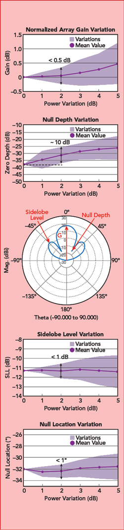
Figure 2 Effect of random element gain variation on beam shape.
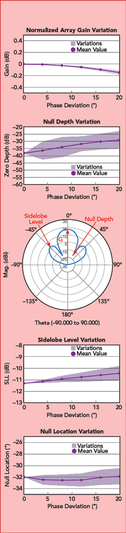
Figure 3 Effect of random element phase variation on beam shape.
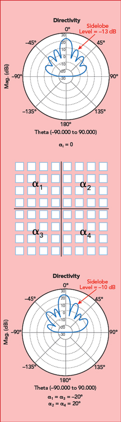
Figure 4 Phase variation among subarrays will degrade gain and sidelobes.
Larger array sizes, such as 256 elements, are being designed to transmit a single beam using all the elements or four simultaneous beams, each with 64 elements. When the subarrays are combined to serve a single user, phase variation among the subarrays greater than 5 degrees will require the subarrays be calibrated. Figure 4 shows an example where a ±20 degree phase differences among the subarrays degrades the antenna gain by 0.5 dB and the sidelobe level by 3 dB. This is a practical concern, which has been identified with 256 element arrays currently deployed. Higher sidelobe levels increase the probability of interference, which will reduce the maximum cell density in a network. Decreased gain reduces a radio’s range, which will increase the cost to cover a given area.
HIGHEST INTEGRATION
Given mmWave IC design challenges, the industry has generally not developed beamformers with more than four or eight channels. However, lower density beamformers shift design complexity to the customer: added high frequency routing, supply and control signaling and operational inefficiencies related to a more complex supply chain. ADI’s heritage in mmWave technology offers world-class system design expertise and applications support, helping customers optimize the system RF, thermal, power and signal routing.
The adoption of mmWave for 5G active antenna arrays with stringent high volume cost requirements will accelerate as early commercial deployments ramp into production and 5G becomes integral to the consumer’s life. This technology will be foundational to provide ubiquitous, secure, high capacity connectivity at a low cost-per-bit. Continuing innovations will enable advanced signal processing functions to be integrated into the chipset. ADI recently demonstrated an antenna-in-package design incorporating the entire mmWave front-end in a single 20 mm x 20 mm surface-mount IC. This broadband, high density packaging IP is compatible with all relevant silicon process technologies, supporting the integration of digital processing such as crest factor reduction, digital predistortion and array calibration.
Analog Devices Inc.
Norwood, Mass.
www.analog.com