
S-Band active aperture phased array radars require multiple power amplifiers (PA) producing sufficient RF output power with high power-added efficiency (PAE). GaN technology is now the preferred choice for many of these applications. This article describes the design, realization and evaluation of a PA for S-Band radar using a GaN power transistor from Qorvo. The QPD1020 has hybrid input matching, i.e., a GaN transistor with an internal passive input matching network fabricated on a cost-effective GaAs process. It offers the cost advantages and flexibility of a discrete transistor with many of the space and development time savings of a MMIC solution. The input of the device is internally matched to 50 Ω across 2.7 to 3.5 GHz. As most S-Band radars will only use a portion of this band, the PA output match may be optimized for either output power or PAE across the intended operating band. PAs have been designed to optimize performance across 2.7 to 3.1 or 3.1 to 3.5 GHz by changing only the component values of the RF matching networks. This approach shortens development time compared to a discrete power bar solution.
Active aperture phased array radars require high efficiency solid-state PAs capable of output power of 10s of W. In recent years, GaN on SiC technology has fulfilled this need at L-, S- and X-Band. However, the RF radar engineer still has to select an appropriate form factor for the PA based on specific radar requirements, including adaptability and cost.
This article first reviews the advantages of phased array radar and discusses the passive and active aperture architectures. The requirements of the solid-state PA in an active aperture phased array radar are outlined, showing how a hybrid input matched transistor helps address these. The design of two PAs - “upper” and ”lower” band variants - is discussed, including the measured results. The lower band PA was tuned for 2.7 to 3.1 GHz, the upper band for 3.1 to 3.5 GHz. The transistor used for both bands is the same: the Qorvo QPD1020, with an internal input match covering 2.7 to 3.5 GHz.
PHASED ARRAY RADAR
Compared to the historic radar with a rotating antenna, a phased array enables electronic beam steering, meaning the direction of the beam is steered without mechanically positioning the antenna. The beam is positioned much more rapidly using electronic rather than mechanical steering; as such, the radar can quickly switch between multiple targets and generate multiple independent beams.1 Although the phased array radar has significant technical benefits, it is more expensive and requires a longer development time compared to the historic mechanical radar.
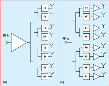
Figure 1 Passive (a) and active (b) aperture phased arrays.
A phased array radar can be implemented as a passive or active aperture (see Figure 1). For simplicity, only the transmit (Tx) path is considered. In a passive aperture, one high-power transmitter is used with a power distribution network feeding the individual elements. The phase at each element is controlled by a phase shifter placed before each antenna. In an active aperture phased array, each element has its own, lower power PA.
When phased array radars were first developed, the passive aperture architecture was preferred, as high-power, high efficiency vacuum tube amplifiers were available that could feed all the antenna elements. In contrast, the solid-state amplifiers used in active aperture radars had relatively low power and efficiency. However, the passive aperture architecture has a number of disadvantages. Phase shifters capable of handling high-power are required, and the loss of the distribution network degrades the overall transmitter efficiency.
In an active aperture topology, the phase shifter is placed before the amplifier, reducing the power handling requirement of the phase shifter. A power distribution network is still required for the active aperture array; however, it only handles relatively modest power levels and does not affect the output efficiency of the PA. The active aperture architecture also offers better redundancy than the passive aperture. If the passive aperture amplifier - typically a vacuum tube - fails, the entire array becomes non-functional. In comparison, if a single PA fails in an active aperture array with hundreds or thousands of elements, the radar continues to function, almost unaffected by the PA failure.
The main limitation of the active aperture array - the relatively low-power and efficiency of solid-state amplifiers - has been largely addressed by GaN technology. This wide bandgap semiconductor operates at higher voltages, hence can achieve higher power density and efficiency than, for example, GaAs at S-Band.
Active phased array radars place many challenging requirements on the PA. When determining the specifications for a GaN PA used in an active aperture phased array radar, the requirements of the system must be carefully considered:
- Printed circuit board (PCB) area can be very limited in a phased array radar, where the radiating elements are spaced one-half wavelength apart.
- The frequency of operation may vary, depending on the particular radar. For example, at S-Band it may not be necessary to operate across the full 2.7 to 3.5 GHz, which provides the opportunity to optimize performance for a particular portion of the frequency band.
- The available DC power for a radar system also varies depending on application. For example, power and cooling will be relatively unconstrained for a fixed ground radar compared to a vehicle-mounted system. In the former case, it may be preferable to optimize the PA for output power to increase range at the expense of DC power consumption and a more complicated cooling system. In the latter case, the PA could be optimized for PAE to minimize power consumption and simplify cooling requirements.
- Another important consideration is in-band stability. In some applications, it may be desirable to add more stability margin, if the PA is expected to operate at very low temperatures or if the impedances seen by the PA are undefined or unpredictable. In other applications, the terminating impedances may be well defined and the K-factor can be reduced to increase gain.
For a radar system developer, it is desirable to optimize each individual radar to the set of requirements; however, this requires a lot of engineering effort and increases the development time and cost. The ability to tune a specific transistor to address particular radar requirements provides the designer with flexibility without requiring new components to be procured and qualified.
PA DESIGN
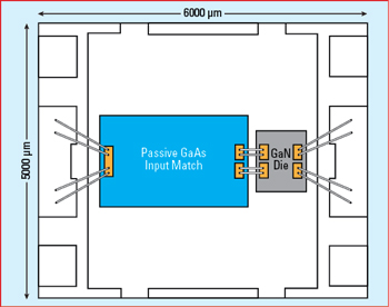
Figure 2 Internal layout of the QPD1020 GaN transistor with hybrid input matching.
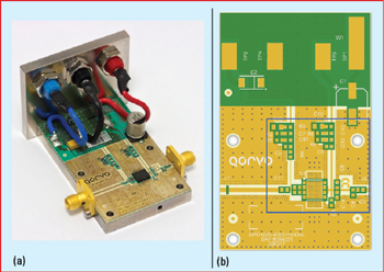
Figure 3 PA evaluation board (a) and PCB layout (b). The design includes both upper and lower band variants; the main circuit area is outlined in blue.
A MMIC provides high levels of performance and only requires a small PCB area. A MMIC also requires minimal design effort from the radar designer: once a suitable MMIC is chosen, it is only necessary to provide the appropriate low frequency decoupling and ensure the package attachment to the PCB provides a reliable electrical ground and thermally conductive path. However, the frequency range and output match of the MMIC is fixed, offering no ability to quickly retune for different requirements. At the other end, a PA based on discrete power bars and surface-mount (SMT) matching components offers high flexibility, at the expense of PCB area, increased development time and increased assembly cost.
A hybrid input matched transistor is a good compromise: more compact than a discrete PCB solution with greater design flexibility than a MMIC. It is also less expensive than a GaN MMIC while providing the performance required by a modern active aperture phased array radar. The radar designer’s job is simplified by only having to retune the PA using SMT component changes. Figure 2 shows the internal layout of the Qorvo QPD1020 transistor. The GaN on SiC power transistor is fabricated on a 0.25 μm, high voltage GaN process, which can be operated at drain bias up to 50 V. The passive input matching circuit die, fabricated on a Qorvo GaAs process, is designed to cover 2.7 to 3.5 GHz and provide some in-band stability. Assembled in a plastic overmold package reduces cost, compared to an air cavity or metal-ceramic package, an important consideration when the transistors will be used in high volume.
Figure 3 shows the PA test fixture and evaluation board. The PCB was constructed from Rogers 4350B laminate with a thickness of 20 mils and was bonded to an aluminum carrier, with an aluminum sidewall with banana plugs added for testing and evaluation. The same PCB layout was used for both the lower and upper band PAs. The SMT components that tune the frequency include a parallel RC network on the input and several shunt capacitors on the output. While designing and fabricating a new PCB layout with modified SMT component positions offers the maximum control over performance, it is considerably more expensive and time consuming.
The PCB measures 40.1 mm x 63 mm; however, the area for RF matching and low frequency decoupling measures only 26.7 mm x 24.1 mm. Copper-filled vias in the PCB provide a good electrical ground and thermal path for the transistor. High quality 0603-sized capacitors are used to reduce unit-to-unit variation. With the 50 V supply voltage, the capacitors must have a suitable breakdown voltage.
The PA shown in Figure 3 was originally designed for the 2.7 to 3.1 GHz band,2 using transistor load-pull data and S-parameters and an EM simulation of the PCB layout. The same PA was subsequently retuned to cover 3.1 to 3.5 GHz. For optimum performance, a small shift in position of the first decoupling capacitors helped shift the response up in frequency. To demonstrate the adaptability of the hybrid input matched approach, the lower band PA was tuned for PAE and the upper band PA for output power.
MEASURED PERFORMANCE
All measurements include the losses from the PCB and 3.5 mm connectors.
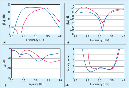
Figure 4 Measured small-signal gain (a), |S11| (b), |S22| (c) and stability factor (d) across the lower (blue) and upper (red) bands.
Figure 4 shows the measured small-signal performance of the two PA variants. The lower band was tuned to 2.7 to 3.1 GHz, the upper band to 3.1 to 3.5 GHz. The upper band PA has a positive gain slope, which can be desirable in some applications, as it reduces the need for a gain equalizer. As the input return loss is largely determined by the GaAs passive die within the package, the input return losses of the two variants are similar. The output return loss is set by the PCB output matching network; there is a considerable shift between the variants, corresponding to the desired frequency bands. The stability factor is higher for the upper band PA than the lower band PA. These measurements show how stability factor can be traded for small-signal gain. As discussed, the required stability factor depends on the operating environment of the radar.
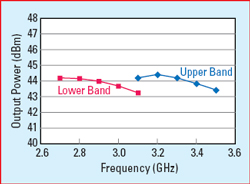
Figure 5 PA output power at P3dB, including evaluation board losses.
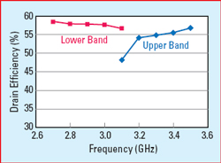
Figure 6 PA drain efficiency at P3dB, including evaluation board losses.
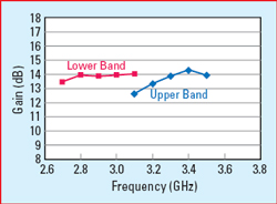
Figure 7 PA gain at P3dB, including evaluation board losses.
The two PAs were measured under pulsed large-signal conditions using a 128 μs pulse-width signal with a 10 percent duty cycle. Figure 5 shows the output power at 3 dB compression (P3dB) for both PAs. Both produce greater than 43 dBm (20 W) output power within their target frequency bands, with a typical P3dB of 44 dBm for the upper band PA. Figure 6 shows the respective PAE at 3 dB compression, including the output losses of the device package, PCB matching networks and SMA connectors. As noted, the lower band PA was tuned for optimum PAE and the upper band PA for P3dB. For comparison, the estimated drain efficiency of the GaN transistor is 64 percent. The efficiency of the upper band PA rolls off at 3.1 GHz; further tuning may improve it. The gain at 3 dB compression is plotted in Figure 7. As with the small-signal gain, the upper band PA shows a positive gain slope, while the gain of the lower band variant is almost flat across the operating band.
CONCLUSION
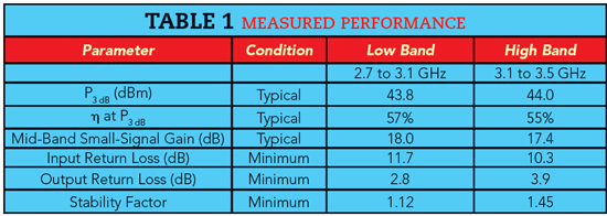
Active aperture phased array radars have many technical advantages over the passive aperture architecture; however, they require high-power and high efficiency PAs. The hybrid input matched transistor offers an adaptable and cost-effective solution which reduces development time and PCB area compared to a discrete power bar approach, yet allows the RF radar engineer to retune performance to meet the specific needs of the radar system. Two example PAs using the QPD1020 GaN transistor were designed and measured, achieving good performance (see Table 1). The same transistor and power amplifier layout can be retuned for a different frequency band, with the output match designed to optimize output power, PAE or a trade between the two.
References
- M. I. Skolnik, “Introduction to Radar Systems, 3rd ed.,” McGraw Hill, New York, 2001.
- R. Smith, L. Devlin, R. Santhakumar and R. Martin, “Cost-Effective Hybrid Input-Matched GaN Transistor for S-band Radar Applications,” ARMMS Conference, April 2018.