
The 3.5 GHz band is emerging as prime 4G and 5G spectral real estate around the globe. Radio interfaces are evolving through LTE-Advanced and LTE-Advanced Pro, raising the bar on base station power amplifier (PA) capability and performance. Instantaneous signal bandwidth is the key to a suitable solution. This article outlines the fundamentals of PA design for a symmetrical, wideband Doherty using load-pull and introduces concepts such as “Doherty friendliness” and “digital predistortion (DPD) compatibility.” The design example of a wideband Doherty PA (DPA) demonstrates a solution suitable for 3.5 GHz LTE-Advanced: a two-stage LDMOS DPA delivering 6.61 W average (35 W peak) at 37 percent efficiency, with 24.5 dB gain and over 300 MHz instantaneous signal bandwidth.
The RF carrier is the virtual packhorse of the cellular network. Today’s 4G LTE-Advanced network operates with the concept that a team of packhorses, in aggregate, carry a heavier burden. With LTE-Advanced Pro, the next evolutionary step in cellular network technology, multiple packhorses are tied together: some we own, some we borrow when needed. The beasts we borrow come from a shared pool, such as the Citizen’s Broadband Radio Service (CBRS) spectrum.
The U.S. CBRS spectrum - 3550 to 3700 MHz - is open to the public and administered via a central server for “dynamic shared use,” either within a building or outdoors via small cells. Mobile network operators in the U.S. are thrilled about this new cost-effective option for LTE-Advanced network capacity expansion. In China and other leading 5G nations, the 3.5 GHz band - 3400 to 3800 MHz - will become primary licensed spectral real estate for 5G.
LTE-Advanced Pro was introduced with 3GPP Release 13 and builds on LTE-Advanced from 3GPP Release 10. LTE-Advanced accommodates five simultaneous carriers, aggregating 100 MHz bandwidth. With LTE-Advance Pro, the capacity jumps to 32 simultaneous carriers, mixing licensed and shared spectrum with higher-order modulation and higher-order MIMO, using up to 640 MHz aggregate bandwidth. These capabilities push the requirement for instantaneous signal bandwidth (ISBW), the maximum modulated signal bandwidth, ever higher in the radio interface, which is particularly challenging for the RF PA (RFPA) design.
RFPA technology, on its own, is unable to address the linearity requirements of LTE-Advanced over wide bandwidths. Using adaptive numerical methods, DPD provides the necessary bridge to the performance required of higher-order modulation and wider signal bandwidth. The RFPA is engineered to dovetail with the DPD system, a task that would be quite difficult if the RFPA and DPD were not designed for compatibility - a quality RFPA designers call “DPD compatibility.” More on this in a bit.
The following discussion will demonstrate the fundamentals of DPA design based on a device uniquely suited for LTE-Advanced applications, a solution using NXP’s A3I35D025WN, a two-stage LDMOS DPA that delivers 3.4 W average (45.2 W peak) with 34 percent efficiency, 24.5 dB gain and greater than 300 MHz instantaneous signal bandwidth (see Figure 1).
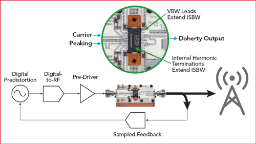
Figure 1 Wideband Doherty PA with DPD.
DPA DESIGN
The DPA is the current topology of choice for efficient, high power RF amplifiers (see Figure 2). The “trick” of the Doherty configuration is: At lower signal power, the peaking drain is in an off state and the carrier path is providing the full power gain, as efficiently as possible based on the bias. As the signal level increases, the peaking transistor turns on, changing the impedance it presents to the Doherty combining node. At full power, the carrier’s performance is pulled from optimal efficiency to maximum power. However, the magic is that none of the energy used to pull the carrier drain is wasted.
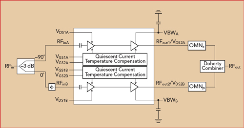
Figure 2 Functional block diagram of the NXP A3I35D025WN Doherty PA.
The designer selects the load impedance targets for the carrier and peaking amplifiers for the two modes of Doherty operation: full power and the peaking path off. Zopt reflects the full power mode, corresponding to the maximum output power, and Zmod reflects the peaking off mode, corresponding to optimal efficiency. Zopt is the target drain impedance at the carrier and peaking drains in full power mode. In this mode, the carrier and peaking paths combine constructively at the Doherty combining node, and the peaking output is actively load-pulling the carrier output toward maximal output power. Zmod is the target drain impedance at the carrier drain in the peaking off mode. In this mode, the peaking path is in its off state and should not be loading the Doherty combination node significantly.
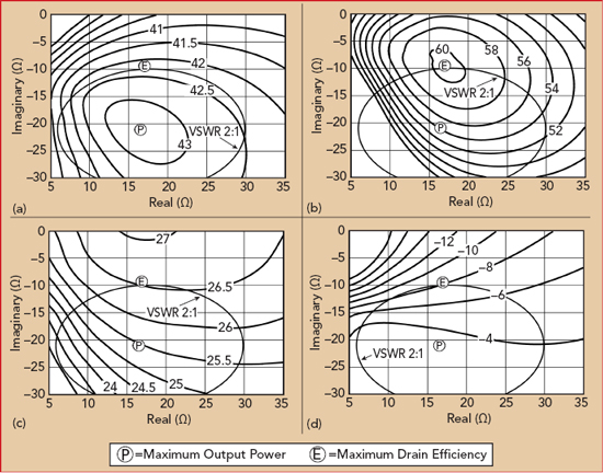
Figure 3 3600 MHz load-pull contours: output power (a), drain efficiency (b), gain (c) and AM/PM at 3 dB compression (d).
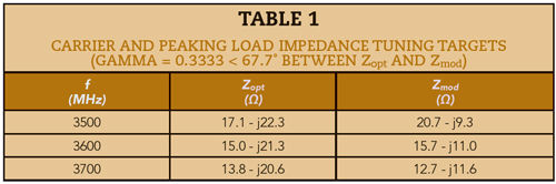
These impedances are selected from the load-pull contours at the predefined bias settings at the band-center and band-edge frequencies (see Figure 3 and Table 1). Note the gamma spacing between the Zopt and Zmod points: |gamma| = 0.3333 or 2:1 VSWR. This spacing corresponds nicely with the 2:1 VSWR load modulation of the carrier drain with a symmetrical Doherty - the first characteristic which indicates the Doherty friendliness of the device. Also note any significant gradient in output power, efficiency, gain and AM-to-PM vs. load impedance in and around the Zopt and Zmod points, i.e., within 2:1 VSWR. There should be no significant gradient in load-pull contours across frequency; the lack of any significant pitch also reflects Doherty friendliness for wideband applications.
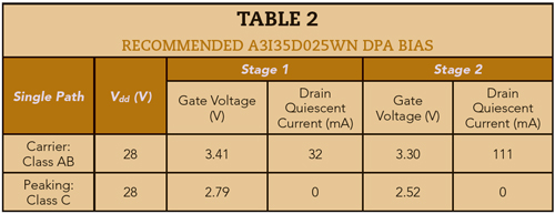
The best starting point for the optimal device bias is at or near class AB, as defined in the product datasheet (see Table 2). As noted, in the Doherty configuration, the carrier amplifier will be operated in class AB and the peaking path in or near class C. Thermal tracking circuits on the A3I35D025WN DPA regulate the quiescent current over wide temperature variation, and the datasheet specifies the quiescent current accuracy over temperature, gain variation over temperature and output power variation over temperature. Consider using an off-chip temperature monitor if the datasheet specification for variation over temperature is not sufficiently precise for the target application.
ICs specifically configured to bias LDMOS Doherty circuits are available, such as TI’s AMC7834 or ADI’s AD7294. In addition to setting the bias, they monitor temperature, current and voltage. The key parameters to monitor and control are the carrier amplifier quiescent current, maximum channel or junction temperature and accommodating part-to-part variation in the transistor pinch-off voltage.