
The response of the circuit in Figure 7 can be seen in Figures 8 and 9. Figure 8 illustrates the effect of changing the gain around the loop, from positive for Q enhancement, to negative for Q spoiling. Figure 9 shows the response if the loop gain is held constant, and the resonator is tuned. The level of Q enhancement remains constant, and the resonant frequency is tuned. It should be noted that the throughput gain of the regenerative filter increases proportionally with Q enhancement, so the plotted responses have been normalized accordingly for better clarity.
Limitations with Conventional Regeneration
Regenerative circuits, such as the ones illustrated here so far are challenging to control. Maximum Q enhancement is achieved near the threshold of instability. To optimize Q enhancement, quenching circuitry has been devised, including circuitry known as Super-Regeneration.2 Super-Regenerative circuits have limited application because of the periodic operation of the quenching circuit.5 Oscillation frequency jumps, and hysteresis, are also problems with regenerative circuits, resulting in unpredictable control characteristics. This has given regeneration a reputation of being finicky and only useful in limited esoteric applications.
New Approach
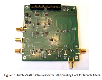
A new circuit has been developed and demonstrates an innovative circuit approach that overcomes these aforementioned limitations. It incorporates multiple passive resonators in the regenerative loop. This approach results in a circuit that behaves as a single pole, and which overcomes issues with control and stability.6 Three resonators in the loop are adequate to ensure controllable and predictable performance. The initial demonstration of this concept was implemented with off the shelf components on an FR4 board, shown in Figure 10. The block diagram is shown in Figure 11. The ATL3 circuit incorporates three resonators, which were implemented with coupled lines on the FR4 board, tunable with varactors. The Q of these internal resonators is 70, but they could be much lower. A Q of 10 is sufficient to realize an ATL3 active resonator with an enhanced Q of greater than 1000. This implies that the filters are attractive for semiconductor implementation. For the first time, compact high performance bandpass filters can be fully integrated on chip. They can operate at any frequency commensurate with the targeted semiconductor technology.

Figure 11 The block diagram of ATL3 active resonator.
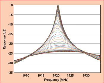
Figure 12 Measured response of ATL3 showing variable Q as loop gain is adjusted.

Figure 13 Frequency tuning ATL3.
The performance of the ATL3 demonstration is illustrated in Figures 12 and 13, showing how Q can be enhanced, as well as how the resonant frequency can be tuned. Repeatable and stable Qs of 2000 have been achieved with this demonstration board. The resonant frequency can be tuned over a relative band of 15 percent which is not a limitation of the ATL3 concept. Rather it is a limitation with this demonstration prototype due to the choice of resonator used. Larger tuning ranges could be achieved with a redesign of the passive resonators and the varactor tuning structure, similar to broad banding VCOs. Further, switches can be used to extend tuning with multiple matching circuits, varactors or resonators.
Control and Calibration
Another attractive feature of this circuit is the capability for self-calibration. This is done by increasing loop gain until the onset of oscillation. This provides an accurate indication of the resonant frequency. It also provides the control point just beyond stable operation. This is possible because, with its three passive resonators, the ATL3 is innately well behaved.
The circuit has three adjustable elements, all digitally controlled via DACs. They are (1) amplifier gain, (2) resonant frequency and (3) phase shift. Amplifier gain adjusts the loop gain. ATL3 has three amplifiers in the forward path, and in the demonstration, they are all controlled together. Resonant frequency is controllable with varactors integrated in coupled-line resonators. The ATL3 has three such resonators in the forward path. They are also controlled together in the ATL3 prototype, but could be controlled individually. The phase shifter provides delays via transmission line sections in nominal 90 degree steps. The phase shift is set to achieve optimum stable control, necessary because of the total electrical length of the loop. In a compact IC implementation, the phase shifter can be designed out.
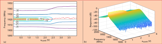
Figure 14 Response of ATL3 as loop gain is varied with acont, where lower voltage result in higher loop gain: (a) contour plot, (b) 3D plot.
The calibration and control of the circuit can be seen in Figure 14. Figure 14a shows response contours for the ATL3 as gain control, denoted by acont, is varied. As acont is increased, loop gain is decreased. Figure 14b shows the same data, plotted in 3D. As loop gain is increased, by reducing acont, the ATL3 reaches the onset of oscillation at about 2 V. For lower values of acont, from 0 to 2 V, is the unstable region where the ATL3 self-oscillates, on the left side of the plot. For acont larger than 2 V the loop gain is less, and ATL3 is stable. A key point of this figure is the dashed red line which indicates the peak frequency response in the stable region and the oscillation frequency in the unstable region. Note that the self-oscillation frequency of the unstable region corresponds precisely with the peak filter response in the stable region. This is the key for self-calibration, so that the ATL3 circuit can self-calibrate autonomously without outside assistance. Further, the frequency variation as a deviation of the red dashed line as a function of acont, is much less than 1 percent. This demonstrates the orthogonality of the Q control and frequency control, which in addition to facilitating self-calibration, also simplifies overall filter control.
Linearity and Noise
Since ATL3s are active resonators, they provide gain and consume DC power. Noise and linearity need to be considered in system design. In a multipole filter, with multiple ATL3 active resonators in cascade, power consumption, linearity and noise must be budgeted across the resonators to optimize overall performance.
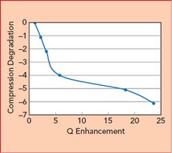
Figure 15 Substantial Q enhancement is measured for Anlotek’s ATL3, with modest degradation in linearity.
The linearity of the ATL3 demonstration board has been evaluated by measurement of AM-AM and AM-PM characteristics. Two tone measurements are impractical with resonators of such high Q and narrowband resonances. Since both forward gain and loop gain increase with Q enhancement, linearity is affected. Figure 15 gives an indication of this mechanism. As the Q enhancement is increased, the sensitivity of the ATL3’s overall gain compression to the gain compression of the loop gain block is also increased. Further, as Q is increased there is more energy storage in the ATL3’s passive resonators, which results in larger voltage swings across the varactor diodes. Careful design is necessary to achieve acceptable gain compression distortion while maintaining low power consumption. This includes budgeting power consumption across the gain blocks, location of gain blocks within the ATL3s and optimizing the system configuration accounting for the ATL3s’ gain.
A theoretical minimum noise figure of the ATL3 is close to 3 dB, due to the fundamental feedback of the loop. This noise figure (NF) limitation can be mitigated with a low noise gain block in front of the ATL3. Hence, with application specific design, the effective NF can be minimized to the point that it is not relevant. The current ATL3 demonstration board described in this work was designed for objectives other than low noise. This is evident from the block diagram of Figure 11. Here the input signal feeds directly into a forward path of a lossy splitter and lossy resonators followed by buffer gain blocks. Further, the gain blocks do not provide sufficient gain to offset accumulated losses, leading to a high NF. If the loop was arranged differently, with the gain block in the forward path and the resonators in the feedback path, then the overall NF would approach that of the theoretical 3 dB. The next step is designing such a filter as an IC.
Looking Forward
The 3 pole MP3 filter described in this article was demonstrated by cascading three of our ATL3 active resonators. Higher order filters are readily realized by cascading more ATL3s, so that virtually any conceivable all-pole filter can be synthesized. Multi-band filters can be implemented by parallel combinations of groups of cascaded ATL3s.
Although the ATL3 active resonator demonstration boards are physically large, they need not be so. ATL3 can readily be designed as an integrated circuit, and the circuit elements would be appropriately small. The largest physical area will be needed for the passive resonators. But since it only needs passive resonator Qs on the order of 10, these too would be quite compact. ATL3 can be designed to operate at any frequency consistent with the semiconductor process being used. All that is needed is sufficient gain to overcome resonator loss. At mmWave frequencies the passive resonators will be very small, making ATL3 an attractive candidate for 5G applications, including in beam steered arrays. There is no other compact technology for highly selective filters at microwave frequencies over 6 GHz or for mmWave. This makes Anlotek’s regenerative technology a good candidate for a wide range of applications above 6 GHz.
Summary
The era of semiconductor electronics has seen a constant migration of traditional discrete circuit functions into alternate integrated circuit implementations. Transistor intensive designs have replaced traditional approaches, taking advantage of the small size, low cost and functionality of transistors. This new design technique offers a path for high performance analog filtering that is fully integratable on chip. Stable, agile and highly selective bandpass filters are realizable using only readily integratable low Q resonators, gain blocks and digital control. This circuit has demonstrated the first high performance analog filter technology that is naturally native to integrated circuit technology.
With proper system architecture and circuit design, Anlotek’s filter technology is applicable to a wide range of applications and a wide range of frequencies, from RF through mmWave. With its frequency agility, self-calibration and ease of semiconductor integration, the technology offers system capabilities and flexibility not heretofore available.
As 5G systems and devices roll out, we will see the same crowding of frequency bands witnessed with the growth of 3G and 4G technologies. 5G is pushing to higher frequencies than have been used in earlier systems, beyond the capabilities of the SAW and BAW filter technologies used in those systems. The size and cost of cavity filters limits their utility. Feedback filters are notoriously difficult to stabilize and control at high Q, but this innovation of multiple resonators in the feedback path, provides stability, calibration and control.
References
- E. H. Armstrong, “Some Recent Developments in the Audion Receiver,” Proceedings of the IRE, Vol. 3, No. 3, pp. 215–238, 1915.
- E. H. Armstrong, “Some Recent Developments of Regenerative Circuits,” Proceedings of the IRE, Vol. 10, No. 4, pp. 244–260, 1922.
- W. B. Kuhn, F. W. Stephenson and A. Elshabini-Riad, “A 200 MHz CMOS Q-Enhanced LC Bandpass Filter,” IEEE J. Solid-State Circuits, Vol. 31, No. 8, August 1996, pp. 1112–1122.
- X. He and W. B. Kuhn, “A 2.5 GHz Low-Power, High Dynamic Range, Self-Tuned Q-Enhanced LC Filter in SOI,” IEEE Journal of Solid-State Circuits, Vol. 40, No. 8, August 2005, pp. 1618–1828.
- D. G. Tucker, “The History of Positive Feedback: The Oscillating Audio, the Regenerative Receiver and Other Applications up to Around 1923,” The Radio and Electronic Engineer, Vol. 42, No. 2, February 1972, pp. 69–80.
- U.S. 10,050,604 B2, U.S. Patent, August 14, 2018.