
For many years, digital transceivers have been used in a wide variety of applications, including terrestrial cellular networks, SATCOM, radar-based surveillance and Earth observation and monitoring. Their capabilities will also directly impact the efficiency and system cost of new 5G mobile networks. Traditionally, transceiver systems have used intermediate frequency (IF) architectures for such applications. However, the most recent improvements in the capabilities of high speed data converters enable innovative architectures based on RF sampling, offering a number of benefits and efficiencies at the system level. These include not only SWAP-C, but also time-to-market and flexibility through the capabilities of software-defined radio (SDR) and software-defined microwave (SDM). SDR and SDM enable engineers to address multiple applications with unique system hardware, yet capable of supporting multiple configurations and requirements.
Before examining how the latest generation high speed data converters can help deliver these benefits, it is worth looking at the two transceiver system architectures.
IF ARCHITECTURE
The IF architecture consists of a hardware chain that generates the RF frequency through one or more IF stages. These stages are known as up-converters on the transmit (Tx) path, converting from a lower to a higher frequency, and down-converters on the receive (Rx) path, converting from a higher to a lower frequency. Figure 1 shows this type of architecture with two stages of frequency conversion.
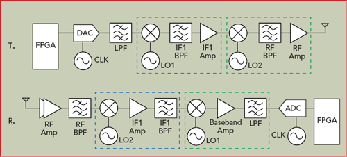
Figure 1 Tx and Rx paths in a transceiver with two up- and two down-converter stages.
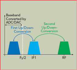
Figure 2 Transceiver frequency plan with two frequency conversions.
The up-converter stage comprises a mixer, driven by a local oscillator (LO), which does the frequency conversion. This is followed by a filter, needed to remove images generated by the mixing process and, sometimes, by the amplification stage. Figure 2 shows the successive conversion steps in this example with two frequency conversion stages. While not discussed in detail here, the image frequencies generated by this process must be filtered to avoid performance degradation through aliasing and power distortion. On the Tx side, the first up-conversion stage converts the baseband or first Nyquist signal to the intermediate frequency IF1, while the second stage converts the signal from IF1 to the RF frequency. The process is reversed on the Rx side (RF frequency to IF1, then IF1 to baseband), and the signal is converted by the analog-to-digital converter (ADC) and then digitally processed for demodulation, for example. The number of frequency converters and choice of IF vary according to the application and are not always the same for Tx and Rx.
The IF architecture was invented during World War I and, since then, has been used extensively, mainly because it was the only solution enabling digital processing of RF signals. The ability to interface between a high frequency RF signal and a data converter handling the baseband remains its main benefit. Because data converter capabilities have, for many years, been limited to low frequency conversion from and to the digital domain, specific analog implementations were needed to use the RF frequency spectrum while taking advantage of increased digital processing power. The primary drawback of this solution is the increase in RF hardware, leading to SWAP-C and performance degradation. Another drawback - harder to identify without considering alternative architectures - is the lack of flexibility, because IF frequencies are fixed by the LO and the data converter input/output frequencies.
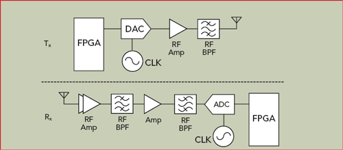
Figure 3 Tx and Rx paths in a transceiver with an RF sampling architecture.
RF SAMPLING ARCHITECTURE
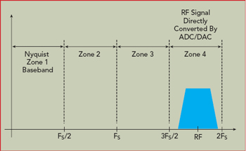
Figure 4 Transceiver frequency plan with two frequency conversions.
Using broadband data converters, RF sampling directly converts the RF signal to the digital domain and removes the up- and down-conversion stages (see Figure 3). RF sampling requires ADC and digital-to-analog converters (DAC) capable of converting signals directly from higher frequencies or Nyquist zones, where a Nyquist zone is a frequency band equal to half of the sampling frequency of the data converter, as defined by the Shannon-Nyquist theorem which is expressed as kFs/2 or (k+1)Fs/2, where k is an integer. Figure 4 illustrates direct sampling of a signal in the fourth Nyquist zone.
RF sampling has long been a key objective to minimize processing in the analog domain. The more done in the digital domain, the greater the flexibility of the system, reusing hardware for multiple applications and providing cumulative savings in time-to-market and qualification costs, as well as reducing risk. In addition to enhanced flexibility, RF sampling can reduce cost and power consumption by eliminating the analog frequency conversion components.
These improvements, made possible over several decades through advancements in data converter technology, provide the justification for many system engineers to adopt RF sampling. The main limitation for RF sampling has been the capability of the data converter. Current high speed converters are capable of meeting the needs of RF sampling up to C- and sometimes X-Band, but performance has not been sufficient to reach the higher frequency bands, such as K-, Ka-, E- and V-Bands, being used for 5G, backhaul and future communications systems.
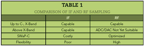
Table 1 compares the IF and RF sampling architectures based on current implementations of these two types. The benefits of RF sampling can be significant but, as with any innovation, RF sampling brings new challenges and requirements, notably the data converters.
DATA CONVERTER SPECS
The performance of today’s transceivers is often limited by the data converter, which plays a critical role interfacing between the digital and analog domains. While many performance requirements need to be considered for the ADC and DAC, regardless of the architecture chosen, the RF sampling architecture places additional focus on key specifications such as the data converter’s analog bandwidth and the DAC output mode capabilities.
Before explaining why these parameters are important in such architectures, and how they drive system capabilities, it is worth reviewing how the Shannon-Nyquist theorem defines the theoretical capabilities of these implementations. The Shannon-Nyquist theorem states that a signal can be reconstructed when the sampling frequency is at least twice the total bandwidth of the signal being sampled, or Fs ≥ 2B, where B = fmax − fmin. This rule is often translated as its first Nyquist equivalent, Fs ≥ 2fmax. This is sufficient for baseband systems; however, to achieve RF sampling at the higher Nyquist zones, the full theorem must be used. With aliasing, the same information is contained in every odd Nyquist zone and reversed in every even Nyquist zone. RF sampling is possible with anti-aliasing filtering around the Nyquist zone of interest, to segregate a single instance of the information.
The first key specification to consider for RF sampling is the ADC/DAC analog bandwidth, which is similar to a low pass filter, limiting the frequency that can be converted with sufficient precision. Figure 5 shows a simple example where the signal above the second Nyquist zone has too much attenuation caused by the bandwidth of the ADC and DAC. It is important to consider the total bandwidth of the analog front-end, as the amplifiers and filters with ADC and DAC will also impact the total bandwidth that can be recovered by the transceiver.
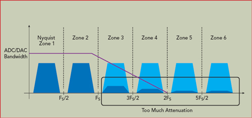
Figure 5 Effect of ADC/DAC analog bandwidth on RF sampling.
Bandwidth is not the sole parameter driving the capability for direct RF sampling. The data converter process and architecture can cause large differences in performance. For example, some ADCs and DACs using CMOS processes specify bandwidths above 6 GHz but have considerable performance degradation as low as 3 to 5 GHz. This is one of the main reasons for using bipolar and BiCMOS processes, as these enable very good performance, even when converting frequencies higher than the converter’s bandwidth. At higher frequency, the bandwidth affects the output power that can be generated, which limits the performance in some applications. However, certain applications do not require very high output power and can work with RF sampling using a device capable of generating frequencies above its specified analog bandwidth. Consider both bandwidth and performance at high frequencies when choosing a data converter for RF sampling.
Another parameter that influences the suitability of a DAC for RF sampling is its output mode capability - more precisely, its effect on the output power it can generate. DACs generate output signals in different output modes, which provide different benefits. For example, the latest generation of DACs offers four different output mode configurations:
- Non-Return to Zero (NRZ) - This mode is the best known and consists of outputting the value of the sample over the full sampling period.
- Return to Zero (RTZ) - This mode is also well known and consists of outputting the value of the sample over half of the sampling period, zero for the other half.
- Narrow Return To Zero (NRTZ) - This output offers a flexible solution between NRZ and RTZ, by outputting the value of the sample over a certain percentage X of the sampling period, surrounded by return to zero for (1 − X)/2 before and after.
- RF - This is the main target for RF sampling and involves outputting the value of the sample for half of the sampling period and the inverted value of the sample for the other half.
The impact of the output mode on the generated output power is better understood when looking at the frequency responses of these modes. The mode should be chosen depending on the Nyquist zone of interest, with the objective of maximizing output power. The choice will depend on the sampling frequency and RF frequency to be generated. For example, a sampling frequency of 6 GSPS and an output frequency in C-Band (between 4 and 8 GHz) equates to either the second or third Nyquist zone, and the RF mode provides the maximum output with only about 5 dB impact on the power. The output mode frequency response depends on the sampling frequency. A DAC at 12 GSPS with output frequency in C-Band would only be up to the early second Nyquist and could be addressed successfully with the NRZ mode.
To be suitable for RF sampling, data converters, in addition to the regular requirements, need to provide sufficient output power and performance up to the target RF frequencies, which translates to analog bandwidth, dynamic performance and output mode (DAC only) specifications. Once appropriate data converters have been identified, the system can be implemented using the RF sampling architecture.
ARCHITECTURE COMPARISON
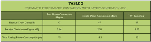
To highlight the differences and benefits of RF sampling over the IF architecture, Teledyne e2v simulated the performance of its latest-generation ADC in three different transceiver configurations: dual-stage IF, single-stage IF and RF sampling architectures. Table 2 shows the estimated power consumption and noise figure. This shows how the system power consumption reduces with every down-conversion stage removed, achieving a reduction of 20 percent between the dual down-converter and RF sampling architectures, while the noise figure performance essentially stays constant. This is because the noise figure performance is mostly determined by the first stage amplification, provided it adds sufficient gain.
Even though the long history of IF architectures in their various forms has made them the default choice for transceivers, new possibilities from advances in data converter performance and capabilities are making the historical architecture less and less relevant for RF applications. RF sampling yields considerable SWAP-C benefits and improves its capabilities with each generation of high speed and high bandwidth converter. The industry will continue to extend the capability of data converters, enabling direct RF sampling at ever higher frequencies.