
This article describes an innovative approach for accurate nonlinear modeling of a high peak power limiter circuit. The modeling approach involves “inside out” modeling of the individual constituent components, which are used to build a composite model. The constituent models include nonlinear models for discrete PIN diodes and linear models for other components, including the coaxial package, capacitors and microstrip circuits. The developed 8 to 18 GHz coaxial limiter model is validated against broadband S-parameter data through 20 GHz and with large-signal power compression measurements at 8 and 13 GHz. The diode models are also validated over temperature at 25°C and 100°C.
Limiter circuits are used extensively in RF/microwave applications, such as the front of receiver chains to protect low noise amplifiers from high-power levels. The limiter’s role is to attenuate the output power to a defined level when high-power signals are received and to let signals pass through the limiter with minimum attenuation when the received power is low.1
A limiter typically consists of PIN diodes and RF inductors in a shunt configuration, with DC blocking capacitors in series. A limiter circuit can consist of a single diode or multiple cascaded diodes separated by quarter wavelength sections of transmission line.2 This work describes a model for a MACOM broadband, high peak power, PIN diode-based limiter (part number 2690-1011).
To obtain an accurate integrated model of the MACOM 2690-1011 PIN limiter, the internal discrete diodes, capacitors, inductors, peripherals (i.e., DC feedlines, bondwires, microstrip circuits) and SMA connectors were measured and modeled. The overall model was then validated with small-signal and large-signal measurements of the limiter at its coaxial reference planes.
DISCRETE DEVICE MODELS
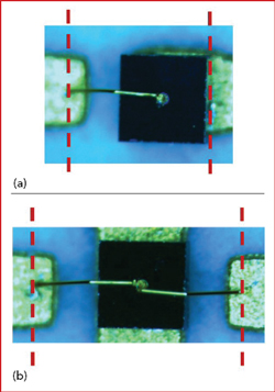
Figure 1 Discrete PIN diode mounted in 2-port series (a) and shunt (b) configurations.
The most important modeling parameters for PIN diodes used in limiters are the intrinsic region thickness, thermal impedance, forward resistance, off-state capacitance, breakdown voltage and minority carrier lifetime. These parameters affect the limiting threshold, power handling, isolation and insertion loss of the limiter. Intrinsic region thickness, breakdown voltage and thermal impedance are directly related to maximum power handling. Minority carrier lifetime determines the recovery time of the limiter. Forward resistance and junction capacitance affect insertion loss and isolation, respectively.3-4
A nonlinear discrete PIN diode model was extracted from a set of measurements that included CV, IV, RF impedance, time domain, S-parameter and large-signal power. The model is based on a Modelithics in-house PIN modeling framework, developed and proven to provide a close fit to broadband linear and nonlinear PIN diode behavior in both the forward and reverse bias regions.5 For fixturing, bond wires connected the parts mounted in series and shunt configurations to 50 Ω input and output feed lines on a 6.6 mil Rogers 4350B test board (see Figure 1).
The IV measurements and modeling results at 25°C and 100°C are shown in Figure 2. The model was fitted to the measured CV and RF impedance characteristics vs. bias at 1 GHz (see Figure 3). Measured and simulated small-signal S-parameters for a 2-port series- and 2-port shunt-mounted diode are shown in Figures 4 and 5, respectively. Although the data is not shown, the PIN model was also validated against large-signal power sweep and time domain transient response measurements. As part of the overall modeling process, a single layer DC blocking capacitor used inside the limiter was characterized and modeled to 30 GHz.
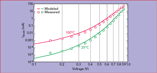
Figure 2 Modeled and measured DC IV characteristics of a discrete PIN diode internal to the limiter.
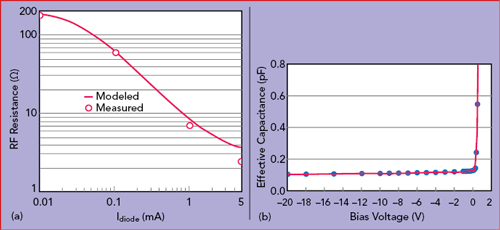
Figure 3 Modeled and measured RF resistance vs. bias (a) and capacitance vs. bias (b) of a discrete PIN diode at 1 GHz and 25°C.
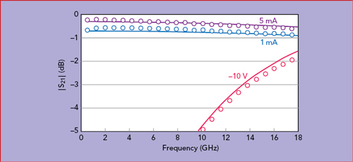
Figure 4 Modeled (solid lines) and measured (symbols) |S21| of a discrete series diode vs. bias at 25°C.
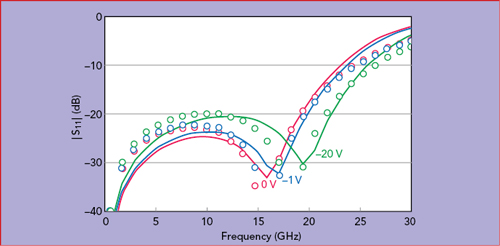
Figure 5 Modeled (solid lines) and measured (symbols) |S11| of a discrete shunt diode vs. bias at 25°C.
LIMITER MODEL
The MACOM 2690-1011 PIN-based nonlinear limiter is specified for 8 to 18 GHz applications and has 2.3 dB insertion loss and 2:1 VSWR, with 1000 W peak power handling (3 W average) and 1000 ns recovery time. The limiter was characterized and modeled using the discrete diode and capacitor models as primary building blocks. Bond wires and capacitors in the discrete component assembly were modeled using Ansys HFSS 3D electromagnetic simulations. These EM models were used to predict the bond wire and capacitor effects in the limiter.

Figure 6 MACOM 2690-1011 PIN limiter.
Multiple samples of the complete coaxial limiter with connectors were characterized with S-parameter and CW power compression measurements. A 3.5 mm short-open-load-through (SOLT) calibration was performed prior to measuring S-parameters from 0.05 to 18 GHz. The measurement and model reference planes were set at the outside edge of the PIN limiter SMA connector, as shown in Figure 6.
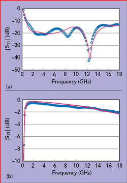
Figure 7 Modeled (solid lines) and measured (symbols) |S11| (a) and |S21| (b) of the MACOM PIN limiter.
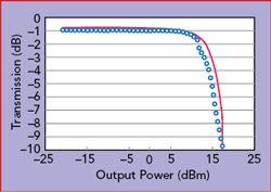
Figure 8 Modeled (solid line) and measured (symbols) transmission vs. output power of the MACOM PIN limiter at 8 GHz and 25°C.
The model tracks the measured S-parameters (see Figure 7), with the modeled performance and measurement showing a maximum insertion loss of 2.3 dB from 1 to 18 GHz, which is consistent with MACOM’s specifications. For large-signal model validation, with the limiter in a series configuration, power testing was performed at 8 and 13 GHz, with input power levels from −20 to 37 dBm and a temperature of 25°C. The large-signal transmission compares closely with the nonlinear model at 8 GHz (see Figure 8). Figure 9 shows the 13 GHz results, validating the high-power limiter model up to 60 dBm input power. The limiter’s performance over temperature reflects the discrete diode’s characteristics versus temperature. While the complete limiter circuit has not yet been validated over temperature, the trend predicted by the model is shown in Figure 10.
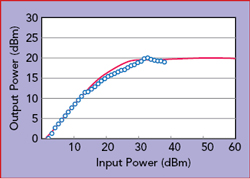
Figure 9 Modeled (solid line) and measured (symbols) output power vs. input power of the MACOM PIN limiter at 13 GHz and 25°C.

Figure 10 Modeled |S21| (a) and output power (b) of the MACOM PIN limiter over temperature, with an input power of 20 dBm.
SUMMARY
PIN limiters are widely used in amplifier receiver chains in the RF/microwave industry. The availability of accurate nonlinear models with advanced simulation features improves the efficiency and cost effectiveness of designing at both the circuit and system levels. Accurate nonlinear models of PIN limiters may be generated using an inside out approach, characterizing, modeling and validating the individual components.
ACKNOWLEDGMENTS
The authors would like to thank Joe Bukowski of MACOM for technical collaboration.
References
- E. Gatard, R. Sommet, P. Bouysse, R. Qu´er´e, M. Stanislawiak and J. M. Bureau, “High Power S-Band Limiter Simulation with a Physics-Based Accurate Nonlinear PIN Diode Model,” Proceedings of the 2nd European Microwave Integrated Circuits Conference, December 2007.
- R. Cory, “PIN Limiter Diodes Effectively Protect Receivers,” EDN Magazine, December 2004.
- R. H. Caverly and G. Hiller, “The Frequency Dependent Impedance of PIN diodes,” IEEE Transactions on Microwave Theory and Techniques, Vol. 37, No. 4, April 1989, pp. 787–790.
- M. U. Nazir, M. Kashif, N. Ahsan and Z. Y. Malik, “PIN Diode Modeling for Simulation and Development of High Power Limiter, Digitally Controlled Phase Shifter and High Isolation SPDT Switch,” 10th International Bhurban Conference on Applied Sciences & Technology, January 2013.
- Modelithics Inc., “Non-Linear Diode Models for Enhanced Simulation Accuracy,” Microwave Journal, Vol. 48, No. 3, March 2005, pp. 152–156.