
A VSWR Meter Using a Power Sensing Termination
EMC Technology Inc.
Cherry Hill, NJ
Transmitted power detection is important in wireless basestation applications in order to insure proper geographical coverage and to meet radiated power regulations. If the power detection is done between the transmitter and antenna then some system performance characteristics may also be measured. Problems with the antenna, antenna cabling and connectors may be detected by measuring the power reflected from defective or inoperable components. Measuring the output power from the transmitter verifies the performance of the transmitter from the oscillator to the final stage of power amplification. Measuring the transmitter output and power reflected from the antenna provides a monitor for the portions of the system that are most susceptible to failure.
CURRENT VSWR DETECTION METHODS
One way to achieve forward and reverse power detection is by using a high power directional coupler with diode detectors on both the input and output coupled ports, as shown in Figure 1 . The ratio of the detected signal levels may then be calculated to determine the reflection coefficient and VSWR. The diodes must be matched to the impedance of the coupler at least at the frequency of operation. Poor impedance matching may result in a reduction in coupler directivity and detection errors. The directivity of the coupler must be sufficient to achieve the desired dynamic range of the detection. For example, a coupler with a directivity of 20 dB will be able to measure a return loss from the antenna no better than 20 dB. In most applications this level of directivity is quite adequate.

There are some practical problems with the diode detector approach. If the two diodes do not have matched responses there will be an error in the detected signal level, and consequently an error in the VSWR calculation.
Using diodes electrically close to the transmitter with no filtering may introduce distortion in wideband systems. Harmonic and intermodulation distortion can re-mix in the transmitter amplifiers and then radiate from the antenna or interfere with the receiver in systems that use a common antenna for both the transmitter and receiver.
As the ambient temperature changes so does the response of the diode detectors. The change in diode response will affect the absolute power level measurement as well as the VSWR if the level of the signal exceeds the square-law region of the diode V-I curve. This response change is a particular problem at high temperatures. Tunnel diodes may be used for detection to reduce the effect of variations with temperature. However, the cost and reliability of the tunnel diodes often drives designers to find alternate means of power detection.
Square-law detection also creates a problem of true RMS detection for high level signals at any temperature. Since signal power is a function of the square of the RF voltage, the diode provides an output voltage that is proportional to the power only as long as the diode remains a squaring device. Of course at high power levels the diode response will depart from the square-law region causing an error in the detected output.
PASSIVE SWR DETECTION
A new device may be used in place of diode detectors to avoid the problems with semiconductors. Together with two, low cost RF switches the Smartload, as shown in Figure 2 , provides true RMS detection, without distortion, over wide temperature and frequency ranges. By switching between the terminations and the Smartload input, part-to-part variations in the Smartload may be eliminated, as well as small variations in device output over time and temperature. Using a single detector also reduces the circuit cost, minimizes PC board space and increases circuit reliability. Reliability is further improved by an order of magnitude over a diode circuit by using the all-passive construction of the Smartload.

WHAT IS THE SMARTLOAD?
The Smartload is a passive, thermistor-based, RMS power detector. In order to detect RF power the Smartload relies on the changes in the resistance of two thermistors as they self-heat due to RF power dissipation in the thermistors. Figure 3 shows a schematic of the Smartload.

The RF signal to be detected is coupled through DC blocking capacitor C1, into a termination that is formed by two parallel-connected thermistors R1 and R2. R1 is a positive temperature coefficient (PTC) type and is connected to RF ground through coupling capacitor C2. R2 is a negative temperature coefficient (NTC) type. Both thermistors are ~ 100 O at 25°C with no RF input power. The parallel resistance of R1 and R2 is approximately 50 O. As the temperature of the thermistors changes with power and/or temperature the value of R1 will increase, while the value of R2 will decrease. The resistance that the RF signal sees remains substantially constant for all conditions. However, the DC voltage at the division between R1 and R2, and supplied by the 5 V supply through the 300 O resistor, will change in proportion to the RMS power dissipated in the thermistors. The Smartload output detects true RMS power over the full frequency and temperature ranges of the device regardless of the signal waveform. A second set of matched thermistors (R3 and R4) is constructed on the same substrate without an RF input point. The differential output between V1 and V2 is compensated for variations in output due to changes in ambient temperature.
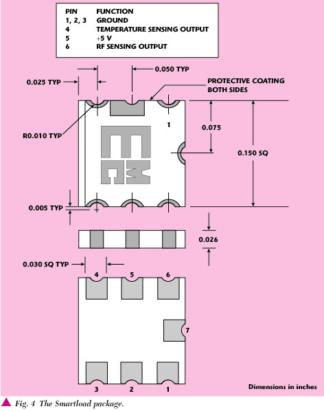
The part is a seven-pin, surface mount technology (SMT) device that may be assembled on a printed circuit board much in the same way as other common SMT components such as resistors, capacitors and integrated circuits. The 3.8-mm square Smartload package is designed for high speed, pick-and-place assembly. Figure 4 shows the Smartload package drawing. An all-thick film construction allows the device to withstand the harsh temperatures and cleaning processes of typical SMT solder re-flow operations. Tape-and-reel packaging is the most common shipping and delivery method for the Smartload.
THE VSWR METER CIRCUIT SCHEMATIC
Figure 5 shows the complete VSWR meter block diagram. Terminated SPDT switches SW1 and SW2 (MA-COM SW-259) are placed on both the forward and reverse coupled ports of the directional coupler. These switches are necessary to compensate for the limited GaAs-FET switch isolation would be limited to the single-switch isolation. A second set of switches SW3 and SW4 (MA-COM AT-246) are cascaded with the first set. SW3 and SW4 are transfer switches with 10 dB attenuators in one of the paths. The attenuators may be used for high level signals to increase the dynamic range of the Smartload. Separate switch drivers (MA-COM SWD-109) control all four switches. The outputs of SW1 and SW2 are connected together and to the RF input of the Smartload.

CALIBRATION
The Smartload may be calibrated for changes in DC offset over time and temperature. To calibrate the device, SW1 and SW2 must be in the termination position. SW3 and SW4 must be transferred with the input switches to the attenuator position and the output switches to the through position. The DC offset of the Smartload may then be recorded for subtraction from later readings.
To measure forward low level power (< 25 dBm) SW1 must be disconnected from the termination while SW2 remains connected to the termination. SW4 must have the input switch connected to the attenuator position and the output switch connected to the through position. SW3 must be transferred to the through path. Forward power may then be measured and the DC offset from step 1 may be subtracted.
To measure forward high level power (< 35 dBm) SW1 must be disconnected from the termination while SW2 remains connected to the termination. SW4 must have the input switch connected to the attenuator position and the output switch connected to the through position. SW3 must be transferred to the attenuator path. Forward power may then be measured and the DC offset from step 1 may be subtracted.
To measure reverse low level power (< 25 dBm) SW2 must be disconnected from the termination while SW1 remains connected to the termination. SW3 must have the input switch connected to the attenuator position and the output switch connected to the through position. SW4 must be transferred to the through path. Reverse power may then be measured and the DC offset from step 1 may be subtracted.
To measure reverse high level power (< 35 dBm) SW2 must be disconnected from the termination while SW1 remains connected to the termination. SW3 must have the input switch connected to the attenuator position and the output switch connected to the through position. SW4 must be transferred to the attenuator path. Reverse power may then be measured and the DC offset from step 1 may be subtracted.
The reflection coefficient (µ ) may be calculated by taking the ratio of the reverse-power measurement to the forward-power measurement. The VSWR may the be calculated using

MEASURED AND CALCULATED RESULTS
The circuit used to test the VSWR meter is shown in Figure 6 . The circuit uses microstrip transmission lines on 0.031", low *r (2.2) polytetrafluoroethylene (PTFE) printed circuit board.

The VSWR meter was tested over temperature using the displayed test circuit. For test purposes the meter was controlled using mechanical switches. In actual use digital switches would be employed. The meter was tested over the range of 40° to 80°C. While the Smartload is specified for operation from 55° to 125°C, the test temperature range was limited by the range of the printed circuit board material and other components.
Figure 7 shows the output voltage from the Smartload, as a function of the power incident at the reverse-power port of the coupler. The output is quite linear over a wide power range. As described in the section on circuit operation, the dynamic range of the sensor may be extended on the low end by using offset calibration, and on the high end by transferring an attenuator in series with the input of the sensor for power levels greater than 25 dBm.
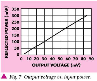
Figure 8 shows the measured and calculated return loss for the VSWR meter as a function of miss-match. The measurements were done using calibrated SMA mismatches that are flat to 6 GHz. The measured and calculated results track quite well.

Figure 9 shows the calculated and measured VSWR for selected frequencies as a function of mismatch. The Smartload operates from 200 MHz to 6 GHz, however, the directional coupler limits the frequency bandwidth of the VSWR meter. Low cost, directional couplers typically have up to octave bandwidths. Broadband couplers may be used to extend the frequency range of operation. Variation in VSWR for very large mismatches may result from differences in coupling with frequency. The coupler may be calibrated by recording the Smartload output for known input power levels over the frequency of operation. The recorded references may then be used to compensate for the coupler frequency response.

Figure 10 shows the measured and calculated VSWR, over the temperature range of 40° to 80°C. The test frequency was 2 GHz. Again, the measured and matched results track well. The temperature range of the VSWR detector may be extended to 55° to 125°C by selecting components equal in operating temperature range to the Smartload.

CONCLUSION
The Smartload-based VSWR meter offers linear power detection over a wide range of power levels and temperatures. The all-passive construction of the device provides lower distortion and higher reliability than active alternatives. The sensor may be implemented using low cost, readily available components. Finally, the performance of the VSWR meter matches the theoretical results over a wide range of reflections, frequencies, and temperatures.
EMC Technology Inc.,
Cherry Hill, NJ (856) 429-7800.