
Introduction
Size, weight and power (SWaP) are important considerations for designers developing equipment for military communications and phased array radar applications. Highly integrated transceivers offer a number of benefits to discrete architectures but powering these devices to deliver the expected performance targets requires careful design and product selection. The high performance that the transceivers deliver are in part based around system calibrations that are run at initialization. It is critical that the power supply for the transceivers both be low noise, but also be sized to handle the power consumption required during the calibration and initialization phase, as well as during the operational phase. Compact high-performance power solutions are readily available to address and meet these challenges. In this short article, we give some suggested approaches to help navigate through the hundreds of possible product configurations.
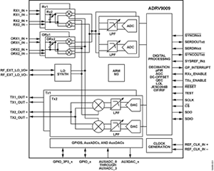
Figure 1 ADRV9009 Wideband Transceiver.
Outline of power requirements for ADRV9009
The ADRV9009 transceiver requires five voltage supplies, 1.3 V analog, 1.3 V digital, 1.8 V, 2.5 V for the interface and a 3.3 V rail. As mentioned in the introduction, ensuring the power rails can deliver sufficient current during the initialization phase is vital as this may exceed the normal operating mode consumption by a considerable margin. Table 1 provides a summary of the requirements; more detailed information is available on request.
|
Voltage Rail |
Initialization Current |
Operating Current* |
|
1.3 V Analog |
2.2 A |
1.2 to 1.9 A |
|
1.3 V Digital |
1.1 A |
0.4 to 1.4 A |
|
1.8 V |
540 mA |
21 to 530 mA |
|
2.5 V |
10 mA |
9.5 mA |
|
3.3 V |
3.1 mA |
3.1 mA |
* Specific mode of operation configured will determine operating current
Designing a Low Noise Power Supply Solution
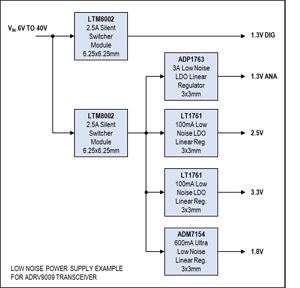
The standard ADRV9009 evaluation board employs a power supply utilizing an ADP5054 Quad Step-Down DC/DC regulator to directly feed the 1.3, 1.8 and 3.3 V rails, with an ADP125 Linear Regulator supplying the 2.5 V interface rail. This configuration provides a basic solution, but to maximize RF performance it is recommended that a lower noise power solution is implemented.
The use of Analog Devices Low EMI Silent Switcher™ technology for the DC/DC conversion may be considered as one option and will provide a well-controlled noise envelope. The Silent Switcher family uses special design and packaging techniques to offer 95 percent efficiency at 2 MHz while easily passing the CISPR 25 Class 5 Peak EMI limits. Silent Switcher 2 adds internal bypass capacitors and an integrated substrate to further improve EMI which is not sensitive to PCB layout, simplifying designs and reducing performance risks. Depending on the power supply load requirements of the application circuit a candidate product could be the LT8650S, Dual Channel 4A, Synchronous Step-Down Silent Switcher 2 DC/DC Regulator. With a 42 V input voltage capability this product also provides some additional design flexibility for higher input voltage rails frequently required in military equipment.
Adding post-regulation to the outputs of the DC/DC convertor will greatly attenuate the output voltage ripple presented to the transceiver, typically circuit designers aim for a 1 percent peak-peak ripple from the DC/DC convertor which by post regulation can be reduced to low µVolt levels using an ultra-low noise LDO linear regulator and good PCB layout techniques. When powering the ADRV9009 transceiver, products to consider are the LT1761, 100 mA, Low Noise, LDO Micropower Regulator in TSOT-23 for the 2.5 and 3.3 V rails and the ADM7154, 600 mA, Ultra-Low Noise, High PSRR, RF Linear Regulator for the 1.8 V rail. For the 1.3 V analog rail the ADP1763, 3 A Low Noise, CMOS Linear Regulator offers some margin for current derating policies if required and occupies a compact 3 mm x 3 mm PCB footprint.
Additional Switching Regulator Considerations
One of the considerations in powering the ADRV9009 Transceiver is that it presents a mix of load requirements that make the power supply difficult to optimize with a highly-integrated product such as the ADP5054, Quad DC/DC Controller/Regulator. Specifically, the light loads of the 2.5 and 3.3 V rails require that the ADP5054 is set to operate in Forced PWM mode, this ensures the regulator operates in its lowest noise mode, this does lead to poorer efficiency at light loads.
Ideally for lower noise, switching regulators supplies should be designed to operate in continuous conduction mode and typically there is a sweet spot operating at around 50 to 70 percent of the full load rating. To maintain continuous conduction with low currents the minimum inductor size must be increased and can become infeasibly large, conflicting with the aims of reducing SWaP. Therefore, these low current rails are better implemented with linear regulators as previously discussed.
Reducing Power Supply Size
We can combine the performance advantage of Silent Switcher technology with µModule Regulator packaging to optimize the power supply solution size through use of products such as the LTM8002, this provides a complete 40 V, 2.5 A switching regulator together with magnetics and passives in a thermally efficient 6.25 mm x 6.2 5mm footprint. It features the Silent Switcher architecture, FMEA pinout and -40ºC to +150ºC operating temperature range.
Alternatively if small solution size is critical then one LTM4622, Dual Ultra-Thin 2.5 A Step-Down DC/DC μModule Regulator in the same 6.25 mm x 6.25 mm footprint could replace two LTM8002 μModule Regulators. The LTM4622 also has an additional feature to select forced continuous mode operation where fixed frequency operation is more critical than low current efficiency, and where the lowest output ripple is desired.
Conclusions
To maximize the high performance that the transceivers can deliver it is important to size the power supply to handle the increased load current when running the system calibration during initialization. Furthermore, to optimize the RF performance a low noise power supply is recommended, some ideas have been presented to improve on the evaluation board design and contribute to reductions in SWaP of the system.