
In the world of high-power amplifiers, the desire to increase the amount of power from a single packaged transistor never ends. Moving from amplifiers consisting of multiple, small transistors to a single, large component simplifies assembly and external combining networks, reducing the overall footprint. Responding to this demand for power, Qorvo developed the QPD1025, a 1.8 kW GaN on SiC transistor for L-Band aeronautical radionavigation applications.
Covering 1.0 to 1.1 GHz, the QPD1025 is a dual-channel device. Biased at 65 V, each side delivers a maximum output power of 900 W at 1 GHz (see Figure 1), yielding a combined power of 1.8 kW—currently the highest power GaN transistor on the market. The peak efficiency, measured with load-pull, is 77 percent. Linear gain, measured in the application board, is 21 dB (see Figure 2). The QPD1025 is assembled in a 41 mm x 10 mm NI-1230 package, available in two configurations: eared (QPD1025L) and earless (QPD1025).
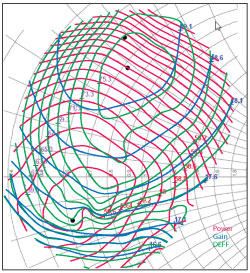
Figure 1 Load-pull contours for a half device, measured at 1 GHz with an RF pulse 100 µs wide at a 10 percent duty cycle. The maximum power is 59.7 dBm, maximum drain efficiency is 77.2 percent and maximum gain is 19.6 dB.
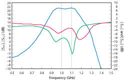
Figure 2 Small-signal S-parameters measured in the evaluation board at 25°C, showing performance outside the 1.0 to 1.1 GHz operating band.
Broadband Performance
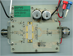
Figure 3 QPD1025L in the application board, which uses in-phase combining.
As transistors get larger, their impedances get lower, which often results in external matching networks difficult to realize and limited in bandwidth. The QPD1025 addresses this problem in two ways. First, using a 65 V drain voltage yields a higher device output impedance than a 50 V device of similar power and technology. The load-pull contours, shown in Figure 1, represent a very manageable output impedance of around 2 Ω per side. Second, on the input, the package contains a single stage prematch that both improves stability and provides a “friendlier” input impedance. These features allow comparatively broadband board designs without having to resort to high dielectric substrates, reflected by the broadband performance in Figure 2.
Combining Flexibility
The dual-channel configuration of the QPD1025 enables multiple amplifier options. The application board, shown in Figure 3, uses in-phase combining, which is compact and low loss. A balanced configuration can be designed using the appropriately-sized hybrid couplers. This architecture affords more isolation between the channels and cancellation of even-order harmonics. Since each side can be biased independently, a symmetric Doherty amplifier design is possible using the correct combining networks.
Stability and Ruggedness
Ensuring the stability of all transistor products is a focus of Qorvo. This starts in the design process with even- and odd-mode simulations with linear models, using loop-gain analysis and parametric measurements. Stability is validated with small-signal measurements at ‐40°C, confirming the QPD1025 is unconditionally stable in the application board. High-power stability is evaluated by looking for spurs better than ‐60 dBc over various VSWR and drive conditions at ‐40°C. The QPD1025 is free of spurs at these strenuous conditions up to 2:1 VSWR. Device stability is largely the product of internal features and requires nothing exotic on the printed circuit board—only a series RC filter at the input and resistors in the gate bias line.
Ruggedness has also been thoroughly tested, demonstrating the QPD1025 survives pulsed testing at 3 dB compression with VSWR loads to 10:1 and overdrive testing to at least 6 dB compression, both measured at 25°C.
Application Board Performance
The application board offered for the QPD1025L uses a compromise match between power and efficiency, trending toward the efficiency match. At room temperature, the drain efficiency is greater than 72 percent from 1 to 1.1 GHz, while the power ranges from 1.3 to 1.5 kW (see Figure 4). Peak dissipation is 460 W, which is below the 500 W CW dissipation limit. Under pulsed conditions, the dissipation limit increases and efficiency may be traded for power. The linear gain is 21 dB at room temperature.
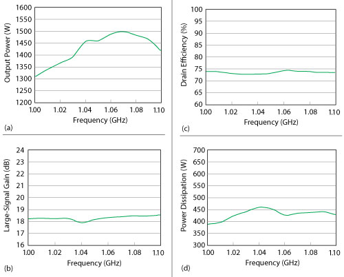
Figure 4 Pulsed performance of the QPD1025 at 25°C and 3 dB gain compression, with an RF pulse 100 µs wide at a 10 percent duty cycle. The application board uses in-phase combining.
The application board substrate uses the industry-standard Rogers RO4350B 20 mil organic substrate on a low-cost, nickel-plated aluminum baseplate. Although the QPD1025 supports independent drain and gate voltages for each channel, the application board ties the gates and drains together with external wires (see Figure 3). The in-phase matching network is quite compact for this power level at 9 cm x 3 cm from the input RC filter to the final output matching capacitor. The overall dimensions of the application board are 11.3 mm x 9.7 mm.
The QPD1025 provides the best combination of power, efficiency and gain available today for applications in the 1.0 to 1.1 GHz band. Its dual-channel design offers manageable impedances, flexibility in amplifier architecture and a compact footprint. Designed with stability, ruggedness and reliability as foremost considerations, the QPD1025 can handle all signal conditions so long as the dissipation limits are respected.
Qorvo Inc.
Greensboro, N.C.
www.qorvo.com