
Analysis of Photonic Bandgap Surfaces Using Ansoft HFSS
Richard Remski
Ansoft Corp.
Grand Prairie, Tx
The microwave industry recently found-new uses for concepts familiar to solid-state designers in the form of photonic band gap (PBG) constructions. PBG constructions offer the ability to produce substrates, ground planes and other structures, which have a forbidden frequency range, or band gap, that does not support electromagnetic waves. This behavior arises from some form of periodicity, in either material characteristics or in a circuit layer, that reacts to electromagnetic fields in much the same way that crystal lattice structures do.
PBG surfaces -- which often become magnetic conductors within their band gaps, much like a corrugated metal plate with the correct characteristics -- have a number of exciting potential uses to the microwave and wireless design world. A few examples include circuit board ground planes (which cannot be excited by long clock traces), novel TEM-mode rectangular waveguides,1 antenna ground planes (which do not image currents and sap antenna gain) and shield surfaces to reduce specific absorption rate (SAR) levels in cellular phone users.
PBG surface structures designed for these applications are currently being modeled with custom algorithms. With the release of Ansoft HFSS 7 and its associated Optimetrics engine, a commercial finite element method (FEM) package is for the first time capable of solving more general categories of PBG devices.
The simplest microwave PBG structures are solid substrates perforated with a rectangular grid of holes, or their complement: a rectangular grid of dielectric rods in air. Assuming a finite number of periods, these structures are easy to model for transmission characteristics in many commercial electromagnetic packages using a waveguide simulator approach shown in Figure 1 . (Five periods in the transmission direction are shown.) Example transmission spectra obtained with Ansoft HFSS for five, six and seven periods of a simple PBG crystal structure are shown in Figure 2 .2


While the described technique suffices for three-dimensional PBG substrates, or "electromagnetic crystals," more directly useful planar or layered PBG structures do not have the necessary degrees of symmetry for analysis in this fashion. Ansoft HFSS Version 7, however, contains the feature set necessary to model these interesting new designs.
OPTIMETRICS AND EIGENMODE SOLVER LEVERAGE ExISTING FEATURES
One of the primary features necessary for efficient modeling of general periodic structures was introduced in Ansoft HFSS 6: the linked boundary condition (LBC). Similar to performing a Floquet-mode expansion, LBCs allow imaging of a unit cell into an infinite array of such cells. However, unlike a waveguide simulator, LBCs permit unconstrained user-assigned field relationships between the master and slave boundaries composing the LBC pair. They allow more than two planes of symmetry, and remove any assumption that the fields on the boundary be forced either tangential to or orthogonal to the boundary faces (as is the case with perfect E and perfect H symmetry). Linked boundary pairs need not always be parallel surfaces, and also need not be perpendicular to other linked boundary pairs, permitting a wide array of lattice arrangements.3
In addition to the capability of defining a lattice with a single unit cell, the new eigenmode solver in HFSS 7 enables direct calculation of the permitted resonance frequencies for a unit cell structure. Computation can be performed over the entire range of field relations between LBC pairs by using Optimetrics. The Optimetrics interface automates the process of altering parametrically the LBC pair's phase relationship to match each value in a table of desired configuration setups and executing each resultant solution. Post-processing capabilities within Optimetrics permit charting of any combination of input vs. output variables, including generation of a display analogous to the dispersion diagram commonly referenced in PBG literature.
The structure shown in Figure 3 is a square array of metallic patches atop a substrate layer (e r = 2.2), tied by central vias to an underlying ground plane.4 This type of PBG structure is of interest to the wireless industry for antenna applications because it cannot support a surface travelling wave within its forbidden band. This behavior permits its use as a ground plane within the designated band, which could enhance -- rather than detract from -- antenna pattern performance. Additionally, the possibility of diffraction around the ground plane edges is also reduced, which should allow for lower SAR levels on the far side of the plane from the antenna where the user's head would be.

A unit cell model representation of this structure (also shown in the diagram) was constructed in Ansoft HFSS 7 and assigned as the nominal problem in an Optimetrics parametric sweep. The top of the model volume is terminated with an anisotropic perfectly matched layer (PML) construction. The variables for the parametric analysis were the phase relationship between each opposing pair of linked boundaries. By varying the phase between the boundaries and calculating the permissible eigensolutions for each phase relationship, a dispersion plot tracing the three sides of the irreducible Brillouin zone (BZ) triangle, shown in Figure 4 , is obtained.

For a plot of possible solution frequencies in the G to x direction, the phase between the first pair of LBCs is held constant at zero and the phase between the second pair is varied from 0° to 180°. For solution frequencies along the x to M direction, the phase between the second pair of walls is held constant at 180° while the phase between the first pair is incremented from 0° to 180°. Finally, for the M to G direction, both relationships are simultaneously varied from 180° back to 0°. Using 10° increments and eliminating the repeated (0°, 0°), (0°, 180°) and (180°, 180°) points result in a total of 54 eigensolution HFSS project setups. All setups are generated for the user by the Optimetrics package following simple construction of a table of parametric combinations. The list of 54 HFSS projects is solved as an automatic batch sequence by the Optimetrics package, and all pertinent results are stored for easy comparison from project to project.
The results of this analysis are shown in Figure 5 . The horizontal axis of each graph represents the changing phase variable for one of the three BZ triangle boundaries, and is analogous to having the wave vector plotted in a true dispersion diagram. Examining the space between the lowest eigensolution frequency for all phase combinations and that of the next highest eigensolution (which falls beneath the light line at either end of the combined plot), a band gap of approximately 10 to 15 GHz is clearly observed. These simulation results closely match those previously reported3 for the same structure, obtained using a custom, non-commercial program.

UC-PBG DISPERSION
Another type of PBG not conducive to analysis with a waveguide simulation is the uniplanar compact (UC) PBG. One such structure is discussed in the literature,5 for which a unit cell model is shown in Figure 6 . The cell dimension is 120 × 120 mils, patch is 100 × 100 mils, inset cutouts are 27.5 × 40.0 mils, centered extension traces are 10 mils wide to end and substrate thickness ( e r = 10.2) is 25 mils.4 As with the prior example, the unit cell structure represents the nominal problem, terminated on top by a PML surface layer. The Optimetrics package is used to vary the phase relationship between the appropriate LBC pair side walls to obtain dispersion data. Figure 7 shows the results for this analysis, which again agree well with those published in the referenced paper and obtained from a custom approach.


FIELD POST-PROCESSING FOR MORE DETAILED ANALYSIS
In many cases, the dispersion diagram is not the only parameter desired from analysis of a PBG structure. Again, Ansoft HFSS and Optimetrics together provide a unique set of capabilities for more extensive evaluation of this class of problems.
Optimetrics permits post-processing of any HFSS-computed quantity as either a parametric sweep output or as part of an optimization goal function. Unlike competing products that only provide data output or optimization toward S parameters or other port quantities, even field analysis results such as antenna patterns, radar cross-section or other derived quantities can be plotted with respect to the setup count or the parametric inputs.
For example, it has already been mentioned that one application of PBG surfaces is as an antenna ground plane. Within the forbidden band not only does the PBG surface not support a travelling surface wave, but it also reflects incident radiation in phase, rather than with a 180° phase shift as would a standard metal ground plane. The region of the frequency band over which the reflected energy adds most constructively (phase shifts of only a few degrees plus or minus from the incident signal) is a subset of the band gap itself. Using Ansoft HFSS and Optimetrics, the reflection phase resulting from an incident wave excitation (averaged on a suitable evaluation plane) can be calculated with respect to incident wave frequency as an output. This capability is made possible by the post processor's Field Calculator, a staple feature of Ansoft HFSS that has been continually maintained and upgraded in each new release.
To illustrate this usage, another example project has been constructed from the designs presented by Sievenpiper et. al.4 and shown in Figure 8 . This hexagonal lattice PBG surface could not be solved in any form using a mere waveguide simulator. However, by modeling a unit cell with LBC side walls and running a parametric sweep using an incident wave excitation at different frequencies, the reflection phase can be calculated directly from field results.

Assuming that the reflected signal is evaluated at a distance d away from the reflection plane, the expected reflection phase from a perfect metal ground plane would be
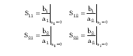
If a PBG structure is placed with its top face the same distance d away from an evaluation plane, the Field Calculator can be used to obtain the average reflection phase at the evaluation plane by calculating
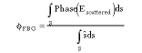
where S is the evaluation surface. (The scattered E field data from an incident wave project are directly available as an input to the Field Calculator following the nominal HFSS solution.)
An integrated macro language allows the calculator routine necessary to obtain  PBG to be automated by recording user operations in the nominal project. Optimetrics then replays the macro for each setup during the solution batch process. The difference between the reference metal plate reflection and the PBG reflection (with an adjustment factor of 180° to center the desired result about zero) is identified in Optimetrics as the final sweep output of interest.
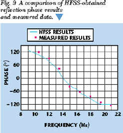
The results of this analysis are shown in Figure 9 , with points extracted from the measured data published in the referenced paper. In this case, the Ansoft HFSS and Optimetrics analysis closely matched results obtained from reflection phase measurements on actual PBG hardware.
CONCLUSION
The exciting study of PBG structures has until now been constrained to modeling via custom algorithms or -- in those few cases where sufficient symmetry exists to use a waveguide simulation approach -- to a finite number of periods in transmission-only models. With the advent of Ansoft HFSS' eigensolution capability and its integration with the parametric analysis capabilities of Optimetrics, the RF designer can now utilize a commercially available, commercially supported software package for more general categories of PBG analysis and design. Analysis can obtain direct finite period transmission, true eigensolution dispersion results and field data for a wide variety of possible lattice shapes and symmetry conditions.
References
1. F.R. Yang, K.P. Ma, Y. Qian and T. Itoh, "A Novel TEM Waveguide Using Uniplanar Compact Photonic-bandgap (UC-PBG) Structure," IEEE Transactions on Microwave Theory and Techniques , Vol. 47, No. 11, November 1999, pp. 20922098.
2. J.D. Shumpert, W.J. Chappell and L.P.B. Katehi, "Parallel-plate Mode Reduction in Conductor-backed Slots Using Electromagnetic Bandgap Substrates," IEEE Transactions on Microwave Theory and Techniques , Vol. 47, No. 11, November 1999, pp. 20992104.
3. I. Bardi and Z. Cendes, "New Directions in HFSS for Designing Microwave Devices," Microwave Journal , Vol. 41, No. 8, August 1998, pp. 2236.
4. D. Sievenpiper, L. Zhang, R.F.J. Broas, N.G. Alexópolous and E. Yablanovitch, "High-impedance Electromagnetic Surfaces with a Forbidden Frequency Band," IEEE Transactions on Microwave Theory and Techniques , Vol. 47, No. 11, November 1999, pp. 20592074.
5. R. Coccioli, F.R. Yang, K.P. Ma and T. Itoh, "Aperture-coupled Patch Antenna on UC-PBG Substrate," IEEE Transactions on Microwave Theory and Techniques , Vol. 47, No. 11, November 1999, pp. 21232130.
Richard T. Remski received his BSEE from the Georgia Institute of Technology, Atlanta, GA, in 1988, having specialized in microwave and antenna design. Before coming to Ansoft, he worked for various aerospace contractors, performing design and analysis tasks on classified airborne antenna and avionics system applications to support the F-16, A-12, B-2, F-22 and V-22 aircraft programs. He has been with Ansoft for nearly three years, where his tasks include technical support, application development, software Q/A and user training.