
High Performance Wideband MMIC Low Noise Amplifiers
This article presents two fabricated 0.25 µm first-pass pHEMT wideband MMIC low noise amplifiers (LNA) covering 1 to 8 GHz and 5 to 20 GHz, respectively. Wideband MMIC LNAs are usually designed with the emphasis on noise figure, which sacrifices the input and output (I/O) SWR. A balance configuration is used to improve the SWR, increasing real estate and complexity. A design to simultaneously achieve low noise, good input SWR across the bandwidth and high gain greater than 20 dB in a single chip solution without using balance topology was achieved. The LNAs' measured performance agreed with prediction. These MMIC LNAs have the best combination of noise figure, I/O SWR, high gain, wide bandwidth and P1dB. The noise figures of the 1 to 8 GHz and 5 to 20 GHz amplifiers are less than 2.6 dB, with I/O SWR less than 2.2.
J.J. Yu and S.T. Chew
DSO National Laboratories
Singapore
Wideband low noise MMICs are used extensively in compact front-end transmit/receive modules and electronic warfare applications. Numerous wideband MMIC LNAs have been designed with techniques utilizing series inductive and shunt feedback in the first stage and subsequent stages, respectively.14 Distributed amplifier topology is used to achieve ultra-wide bandwidth.2,5 A series feedback inductor in the input stage of the MMIC LNA is used to achieve optimum noise figure and low input SWR simultaneously for a single-ended amplifier.6,7 The effect of RLC feedback amplifiers on the bandwidth, SWR, stability and noise figure has been previously demonstrated.811 However, most of these circuits are designed with emphasis on the lowest noise figure possible, allowing the match to degrade with the intention to use balance topology for SWR improvement.
This article demonstrates two optimized LNA designs covering 1 to 8 GHz and 5 to 20 GHz with the objective to provide the best combination of both electrical performance, as in noise figure, high gain and I/O SWR, and circuit real estate. Table 1 shows the performance comparison with other state-of-the-art wideband MMIC LNAs.

MMIC DESIGNS
These two wideband LNAs are designed using a 0.25 µm low noise pHEMT process from United Monolithic Semiconductors, France. The procedure for the general design of an amplifier is noted in Goyal,7 including selection of the circuit topology, device size and number of stages, quiescent point, matching circuit design and layout of the entire circuit. The 1 to 8 GHz amplifier employs reactive input matching with two shunt feedback stages. The 5 to 20 GHz amplifier is a three-stage reactive-matched configuration utilizing series feedback in the first stage and shunt feedback in the last two stages. The LNAs were designed through the use of CAD techniques using HP MDS. The parameters of the FET were simulated using the scaling model.
1 TO 8 GHz LNA
The schematic diagram of the 1 to 8 GHz LNA is shown in Figure 1 . Two 6 * 50 µm HEMTs were used. I-V characteristics of the HEMT devices were simulated to determine a suitable range of bias conditions for proper device operation. The device operates at Vds = 3 V and Ids * 0.21Idss . The negative shunt feedback provides stability for the amplifier and also transforms the input and output impedance to regions to facilitate ease of matching. Although the feedback resistor in the amplifier degrades the noise figure of the amplifier, careful choice of resistor and inductor values achieves wide bandwidth with reasonable noise figure. The feedback amplifier eased inter-stage matching, which was realized using a coupling capacitor and series inductor. Passive lump components were used to reduce the chip size. The design optimization takes into account layout parasitics, bond wires, off-chip input DC blocking and decoupling capacitors. The LNA die and its measured performance are shown in Figures 2 and 3 , respectively. The chip size is 1 mm * 2.2 mm. A 10 pF off-chip capacitor is required for input matching and DC blocking. This capacitor could have been included on-chip but was limited by the specified chip space. Off-chip bypass capacitors of 100 pF are used at the gate and drain.


The measured noise figure of the packaged MMIC is 2.3 dB (typ), with 2.6 dB at 1 GHz. The measured I/O SWR is better than 2.2. At die level, the noise figure is expected to be at least 0.2 dB lower. The amplifier provides 24 dB gain with a flatness of less than ±1.5 dB. It consumes approximately 60 mA and has a minimum P1dB of +14 dBm.
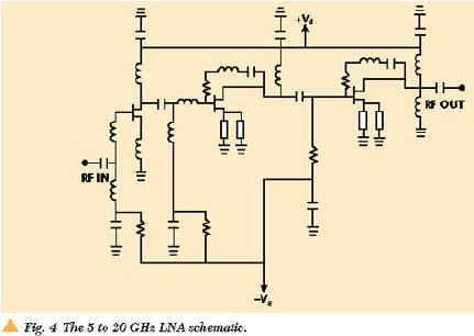
5 TO 20 GHz LNA
Figure 4 shows the schematic diagram of the 5 to 20 GHz LNA. To simplify the biasing scheme, three 4 * 50 µm HEMTs were used and operated at Vds = 3 V and Ids * 0.27Idss . The MMIC is designed to have on-chip DC blocks and bypass capacitors. The series feedback inductor in the first stage of the amplifier improves input SWR, but at the expense of lower power gain at the higher frequency band. A three-element input matching network is optimized for broadband noise figure and input return loss. Short series feedback transmission lines at the source of the second and third stage of the FET were added. The goal was to achieve in-band and out-band stability from DC to 40 GHz. The transmission line length is optimized so that the gain roll-off at high frequency is not significantly large. All biasing networks are part of the matching circuits. The first stage is designed for input match and noise figure, while the second stage is designed for maximum gain and minimum noise figure. The last stage is optimized for maximum gain flatness and output match. Again, lump passive components were optimized to reduce the chip size. The LNA die and its measured performance are shown in Figures 5 and 6 , respectively. The size of the die is 1.5 mm * 2.2 mm.


The on-wafer measured noise figure is less than 2.6 dB up to 18 GHz. A gain of 22 dB with gain flatness of ±1 dB was measured. I/O SWR is better than 2 across the bandwidth. The amplifier consumes approximately 60 mA (typ), and has a minimum P1dB of +6 dBm at 20 GHz. The noise figure above 18 GHz was not measured due to limitations of available equipment.
CONCLUSION
Two MMIC LNAs covering 1 to 8 and 5 to 20 GHz have been designed using a commercial 0.25 µm low noise pHEMT process. The measured noise figure for both chips is better than 2.6 dB with I/O SWR better than 2.2. The LNAs have demonstrated outstanding simultaneous performance in noise figure, high gain and good SWR across the multi-octave bandwidths. These LNAs eliminate the use of balance topology (two-chip solution) to improve the input SWR.
ACKNOWLEDGMENT
The authors wish to thank the Radio Frequency Laboratory and the MMIC's team members, S.J. Koh, P.Y. Chee and Y.W. Kong, for their technical assistance. This project is funded by Directorate of the Research and Development, Singapore, under Project 971279. *
References
11. J. Eisenberg, W. Ou and J. Archer, "A .5 to 6 GHz High Gain Low Noise MMIC Amplifier," IEEE GaAs IC Symposium Proceedings , 1989, pp. 8386.
12. R. Dixit, B. Nelson, W. Jones and J. Carillo, "A family of 2 to 20 GHz Broadband Low Noise ALGaAs HEMMT MMIC Amplifier," IEEE 1989 Microwave and Millimeter-Wave Monolithic Circuits Symposium Proceedings , pp. 1519.
13. J. Panelli, N. Chiang, W. Ou, R. Chan, C. Shih, Y.C. Pao, J. Archer and M. Kumar, "A 2.5 dB Low Noise 6 to 18 GHz HEMT MMIC Amplifier," IEEE 1992 Microwave and Millimeter-Wave Monolithic Circuits Symposium Proceedings , pp. 2124.
14. J. Sanctuary, C.E. Woodin and J. Manning, "Broadband 0.25 Micon Ion-Implant MMIC Low Noise Amplifiers On GaAs," IEEE 1992 Microwave and Millimeter-Wave Monolithic Circuits Symposium Proceedings , pp. 2528.
15. K.W. Kobayashi, W.L. Jones, K. MacGowan, R. Kono and L.S.J. Lee, "A Monolithic DC Temperature Compensation Bias Scheme for Multistage HEMT Integrated Circuits," IEEE Transactions on Microwave Theory and Techniques , Vol. 44, No. 2, February 1996, pp. 261267.
16. R.E. Lehmann and D.D. Heston, "X-Band Monolithic Series Feedback LNA," IEEE Transactions on Microwave Theory and Techniques , Vol. MTT-33, No. 12, December 1985, pp. 15601566.
17. R. Goyal, Monolithic Microwave Integrated Circuits , Artech House, 1989.
18. K.B. Niclas, W.T. Wilser, R.B. Gold and W.R. Hitchens, "The Matched Feedback Amplifier: Ultra-band Microwave Amplification with GaAs MESFETs," IEEE Transactions on Microwave Theory and Techniques , Vol. MTT-28, April 1980,
pp. 285294.
19. C.E. Weitzel and D. Scheitlin, "Single-stage GaAs Monolithic Feedback Amplifiers," IEEE Transactions on Microwave Theory and Techniques , Vol. MTT-33, No. 11, November 1985, pp. 12441249.
10. A.M. Pavio, Jr., "A Network Modeling and Design Method for a 2 to 18 GHz Feedback Amplifier," IEEE Transactions on Microwave Theory and Techniques , Vol. MTT-30, No. 12, December 1982,
pp. 22122215.
11. K. Nicals, "Noise in Broadband GaAs MESFET Amplifier with Parallel Feedback," IEEE Transactions on Microwave Theory and Techniques , Vol. MTT-30, January 1982, pp. 6370.
12. H. Morkner, M. Frank and D. Millicker, "A High Performance 1.5 dB Low Noise GaAs PHEMT MMIC Amplifier for Low Cost 1.5 to 8 GHz Commercial Applications," IEEE Microwave and Millimeter-wave Monolithic Circuits Symposium Proceedings , 1993, pp. 1316.
13. Sanders product catalogue.
 Jong Jen Yu received his B Eng (Hons) from the University of Birmingham, UK, in 1996. He joined DSO National Laboratories, Singapore, in 1996 where he has been engaged in the microwave MMIC circuits and subsystems design. Currently, he is responsible for the development of the compact X-/Ku-band module using LTCC multilayer packaging with integrated embedded passive circuits and the insertion of MMICs. He is a member of the IEEE.
 Siou Teck Chew received his B Eng (Hons) and M Eng from National University of Singapore (NUS) in 1989 and 1993, respectively. He received his PhD from the University of California, Los Angeles, in 1996 under a DTTA scholarship from the Ministry of Defense, Singapore. Since 1989, he has worked at DSO National Laboratories, Singapore. Currently, he is the head of the Radio Frequency Systems Laboratory and a principal member of its technical staff. He oversees the research and development of RF and microwave components and subsystems. His technical interests include active antenna, high power amplifier, filter and nonlinear circuit analysis and design. Chew also is currently an adjunct fellow at NUS, lecturing and supervising research activities. He has published 20 papers and serves as chairman of the IEEE Singapore Chapter for AP/MTT/EMC.