
Since its inception, GaN has shown the potential to transform the RF technology landscape, promising major disruptions across multiple markets. Carefully nurtured from fledgling technology to widescale deployment, GaN’s inherent performance advantages over legacy technologies gained early traction for military applications, where performance far outweighs cost considerations.
GaN’s pathway to mainstream RF commercialization hinges on its ability to support the volume and cost requirements of end applications, including 4G and 5G base stations and emerging RF energy applications—cooking, lighting, industrial heating and drying, medical, pharmaceutical and automotive ignition systems. Cost sensitivities are compounded by the growing need for more integrated components, e.g., MMICs, particularly for dense architectures like massive MIMO antenna systems for 5G base stations. Integrated packaging introduces additional cost that must be offset by lower semiconductor manufacturing costs.
The sheer volume of GaN production required by price-sensitive commercial RF applications and the demands these markets place on the semiconductor supply chain eliminate GaN on SiC as a viable contender, given SiC’s extremely slow ingot growth rate and the present inability to scale GaN on SiC wafer production beyond 6 in. wafer diameter. This leaves GaN on Si technology as the only viable way forward for the commercial development of GaN. However, to meet the volume, cost and surge capacity requirements for mainstream RF commercial markets, GaN on Si production must be ported from III-V compound semiconductor foundries to mainstream CMOS manufacturing lines.
PROCESS DISCIPLINE
In addition to supporting higher production volumes and wafer diameters up to 12 in. on a fully automated platform, CMOS fabs offer the opportunity to exploit strict process controls to achieve more repeatable performance and extremely high line yield, which will drive additional cost reduction. The equipment used in CMOS fabs is more automated and advanced, and the existing silicon manufacturing infrastructure offers opportunities to spread overhead costs for volume microwave GaN on Si production, further reducing the overall cost structure.
To make the jump from III-V to CMOS-based GaN on Si fabrication, considerable effort is required to conform to standard CMOS process nodes—which produce thousands of wafers in a single week. The respective process modules employed in III-V and CMOS wafer fabrication are significantly different. While III-V allows for a degree of flexibility in the workflow, CMOS production flows require strict adherence to distinct and individually optimized modules. There is simply no allowance for individual adjustment to the workflow outside of these highly defined modules.
The rigidity of this approach fulfills an expectation that all processes will work in production the first time and every time—a core philosophy for high volume fabrication. These stringent process controls are designed to produce robust processes that will meet the required fine-line photolithography processes commonly employed in CMOS fabs, with no ability to rework process steps. This approach to wafer fabrication contrasts sharply with typical III-V manufacturing, where in-line wafer scanning electron microscopy is routinely used to adjust fine-line photolithography parameters in an attempt to “inspect in” quality. With CMOS, process disciplines must be airtight from the beginning, or yield and cycle time will suffer.
MAJOR CHALLENGES
Semiconductor surface passivation is a key consideration when transitioning GaN on Si from III-V to CMOS fabrication, given the different surface chemistries each process platform uses. Fortunately, because the properties of GaN on Si HEMT technology are, in many respects, more closely related to silicon than GaAs, industry standard silicon cleans and surface treatments can be used, with more aggressive mixtures of mineral acid/peroxide or hydroxyl/peroxide solutions to prepare the surface for subsequent process steps.
CMOS-based GaN on Si fabrication also takes advantage of advanced atomic layer deposition (ALD) and atomic layer etching (ALE) technologies that are not typically found in III-V fabs. Commercial ALD/ALE systems are capable of depositing high density films with excellent material quality and exceptional uniformity, thickness control and reproducibility, forestalling the possibility of surface damage by avoiding the use of plasma enhancement during the deposition. Films as thin as 50 Å and up to 1.0 μm thickness are routinely applied to silicon with a host of metal oxides and nitrides.
The hardest challenge porting GaN on Si to a CMOS fab is the use of gold for device metallization. Gold has been universally used for all GaN production in III-V fabs because of its low electrical bulk resistivity and excellent electromigration properties. In CMOS fabs, gold is never used in front-end processes because it causes electron recombination traps that destroy the fundamental electron mobility in the device structure. This means that all metallization used in GaN on Si high frequency devices to form the gate —the heart of the device—must be changed to different metals, which impacts the chemicals employed in the process, with significant implications for surface characteristics and overall device performance. Intensive R&D in this area yielded new metallization solutions to overcome this challenge and make it viable for GaN on Si to be produced in CMOS fabs without using gold. This is possible using non-gold ohmic contacts, nickel aluminum gate metallization and interconnects formed from either aluminum or copper.
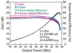
Figure 1 Load-pull measurements at 2.5 GHz, comparing 600 µm test structures fabricated on STMicroelectronics’ 6 in. silicon fab and MACOM’s 4 in. III-V fab.
Wafer thickness is another critical consideration when porting GaN on Si production to a CMOS fab. Wafers produced in III-V fabs for high frequency devices must be as thin as 50 μm, for thermal and electrical performance, and are manually mounted and dismounted. Significant wafer bow—up to several millimeters—creates a high risk of wafer breakage, leading to yield loss and higher cost. In contrast, wafers produced in CMOS fabs can produce wafers in the 50 to 60 μm range, in which the mounting and dismounting is fully automated. Strict process controls were developed for the CMOS fab to ensure that ultra-thin GaN on Si wafers do not suffer from “potato chip” curling and wafer breakage. It is now possible to produce GaN on Si wafers that measure 2 μm in flatness across the 6 in. wafer, by leveraging the CMOS fab processes, and new techniques were developed to allow source vias to be formed from the backside of the GaN on Si wafer in a manner consistent with III-V performance requirements.
PERFORMANCE AND RELIABILITY
MACOM and STMicroelectronics’ (ST) joint development effort to port the GaN on Si process yielded CMOS-manufactured, high frequency GaN on Si devices that exhibit equivalent performance to GaN on Si devices produced in III-V fabs (see Figure 1). RF load-pull of 600 μm test structures at 2.5 GHz achieve essentially identical output power, high frequency gain and power-added efficiency, comparing ST wafer fabrication facilities with a III-V fab.
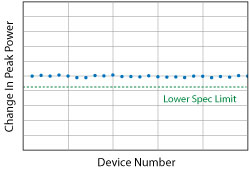
Figure 2 Change in peak output power following HAST on a sample of 25 GaN on Si devices fabricated by STMicroelectronics’ 6 in. silicon fab.
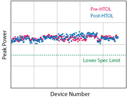
Figure 3 Peak output power before and after HTOL testing for 231 GaN on Si devices fabricated by STMicroelectronics’ 6 in. silicon fab.
In terms of reliability, RF GaN on Si devices produced in the CMOS fab meet the fabs’ reliability standards and, in some cases, outperform the reliability achieved with legacy semiconductor technologies—with a path to meet more demanding reliability requirements. Qualification testing of GaN on Si has been successfully accomplished across a wide range of tests, including highly accelerated stress tests (HAST), high temperature operating life (HTOL), high temperature reverse bias (HTRB), accelerated life testing (ALT) and routine testing for electrostatic discharge (ESD), intermittent operating life (IOL), temperature cycling, mechanical shock and vibration and destructive physical analysis (DPA). Figure 2 shows the stability of RF output power for a population of microwave GaN on Si devices subjected to HAST, and Figure 3 shows minimal change in RF power for 231 devices after HTOL testing.
OPPORTUNITY AWAITS
MACOM and STMicroelectronics collaborated for well over a year to port high frequency GaN on Si production to ST’s CMOS wafer fabs, with sample production planned to begin in 2018. The ability to manufacture microwave GaN on Si devices in a CMOS fab opens the door to a new world of possibilities, including the homogenous integration of GaN and CMOS-based high frequency devices on a single chip. These multi-function RF devices will combine GaN’s power and high frequency benefits with digital control. The R&D to enable this is already underway. High-power digital-to-analog converters, microprocessors and on-wafer wireless transmitters are among the many candidates for single-chip integration.


With the successful porting of RF GaN on Si production to CMOS fabs, GaN on Si technology is uniquely positioned to meet the performance, cost structure, manufacturing capacity and supply chain flexibility requirements of 4G and 5G wireless base station infrastructure, expanding to address solid-state RF energy applications. While the process challenges that were overcome to achieve this goal were myriad and significant, with a small margin for error, the advantages far outweighed the limitations and have enabled a new era in RF technology to begin.