
MICROSTRIP STEPPED-IMPEDANCE LPF
A microstrip stepped-impedance structure provides a way to demonstrate the effectiveness of using a microstrip DGS approach for a LPF without encountering radiation or isolation problems. The circuit consists of low-impedance sections cascaded with high-impedance sections in a repeated pattern. When designed properly, these low- and high-impedance sections produce capacitance and inductance values in different sections of the filter, resulting in a LPF function.
Using a microstrip stepped-impedance format, the difference between the high- and low-impedance sections has an effect on the spurious harmonic performance of the filter. A larger difference between the high- and low-impedance values results in less spurious harmonic content and better isolation in the stopband; however, there are limits to the impedance range that can be realized. For example, if the low-impedance circuit element is too wide, it can cause unwanted resonances that distort filter performance. As a general rule, the width of this structure should be no greater than λ/8 at the frequency of interest. Conversely, high impedances require narrow conductors difficult to fabricate in microstrip. Another general rule is that the minimum microstrip conductor width should be 4 mils or more to provide a circuit design that PCB fabricators can manufacture practically and repeatably.
To achieve high-impedance sections, DGS circuit design features are incorporated to increase the impedance of a circuit section without resulting in conductor widths that are too narrow to fabricate. One of these features is an etched opening in the microstrip ground plane under a narrow conductor. The etched opening significantly increases the substrate thickness in the area, with a resulting increase in impedance.
DGS technology can also be used to enhance filter stopband performance and minimize spurious harmonic responses. This can be done with a DGS that causes a bandstop response in the range of frequencies of the spurious harmonic responses or in the range of frequencies where the filter’s stopband must be improved. In general, to control a filter’s spurious harmonic responses without degrading other filter performance parameters, a narrow bandstop response is created in the frequency range where the harmonic or spurious responses are known to occur. With a DGS, it is typically better to use a wide bandstop configuration within the frequency range of interest.
To better illustrate the benefits of DGS circuit techniques for enhancing the performance of a high-frequency filter, a study of the effects of a DGS on a microstrip stepped-impedance LPF is described. EM modeling is performed using several design approaches and considerations. Physical circuits are fabricated and tested, and the measured performance is compared to the simulated performance from the EM models. To fully understand DGS effects, filters are fabricated using specific combinations of high- and low-εr substrate materials to demonstrate how the choice of circuit materials impacts the performance of a microstrip DGS component.
FILTER DESIGN AND MODELING
The LPF design is based on a Chebyshev transfer function with 0.1 dB ripple and a 3 dB cutoff at 2.2 GHz. Several versions of the filter were designed and fabricated. The first is a reference, designed without a DGS. The second targets the same specifications but with two different DGS approaches and with a particular combination of high-εr and low-εr substrate materials, to form the multilayer structure of the three-copper-layer, microstrip DGS circuit.
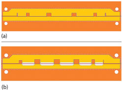
Figure 3 Conventional microstrip stepped-impedance LPF (a), and a circuit with the same design specifications but with DGS openings in copper layer 2 to achieve high-impedance circuit features (b).
The high-εr substrate material used for this study is 8-mil-thick RO4360G2™ laminate from Rogers Corp. It has a design Dk of 6.4. This is the relative permittivity or dielectric constant, εr, as perceived by the circuit (shown as εr1 in Figure 2). The low-εr substrate is a 22-mil-thick 2929 bondply material, also from Rogers. It has a design Dk of 2.9 (shown in Figure 2 as εr2). A benefit of this material combination for the stepped-impedance microstrip DGS design is the use of the high-εr material for the low-impedance sections; low-impedance circuit features are achieved solely by using the higher εr material. When an etched opening is formed in the microstrip ground plane on copper layer 2 to construct the high-impedance circuit features, the circuit behaves as if it is based on a much thicker substrate; the thicker substrate has a combination of εr values from the two different substrate materials with design Dk values of 6.4 and 2.9. Considering the thicknesses of the two substrate materials, the combination yields a composite design Dk of about 3.4. The thicker substrate, with its lower εr value, is used to form a higher impedance circuit feature than is possible with the 8-mil-thick substrate alone.
Figure 3a is a top view of the first LPF circuit design while the same circuit design with ground openings in copper layer 2 is shown in Figure 3b. The color coding shows the top copper layer (copper layer 1, the signal layer) as dark orange and copper layer 2 (the buried microstrip ground plane) as light orange. There are many repetitive grounding vias (shown as white dots) around the periphery of the circuit features. This ensures that the buried ground plane, the top ground plane and the bottom ground plane are consistently grounded together. The bottom ground plane (copper layer 3, shown in white) is below the microstrip buried ground plane (copper layer 2). If Figure 3b were a true microstrip DGS, with only two copper layers, the white area would represent a pathway where energy could radiate to the outside world. With the bottom ground plane (copper layer 3) present, radiated energy is minimized.