
Industrial, scientific and medical applications are migrating from using vacuum tubes to solid-state, requiring RF systems to reach increasingly higher power levels. This move multiplies the number of RF power transistors per system, resulting in combining losses, increased size of power amplifiers and more complex power supply management. As a result, there is an ever-increasing need for higher output power per RF transistor.
Silicon laterally diffused metal oxide semiconductor (LDMOS) is the dominant technology for high-power RF designs. Ten years ago, the industry moved to 50 V drain voltage to achieve 1 kW of output power per transistor. Over time, the 50 V LDMOS technologies improved in ruggedness and power density, last year delivering 1500 W from a single device. That level of CW output power constitutes the upper limit of what can be achieved at 50 V without compromising usability.
This makes a higher voltage technology desirable. Here’s why: There are four ways to boost the output power of an RF transistor. Two involve simply adding more LDMOS periphery on the chip, either by increasing the die size or by increasing the density (i.e., total gate width) of the active silicon on the die. However, both solutions augment the parasitic output capacitance (Cds) of the transistor, making it difficult to match to 50 Ω. The third way is to optimize existing 50 V LDMOS technology further, to increase the power density of LDMOS (i.e., W/mm). This method does not address the fundamental RF transistor design trade-offs. As described in Motorola’s 1991 application note, AN1526, the output resistance is a function of the drain voltage and the output power, shown by the formula

Increasing the output power, P, lowers the output resistance RL. This makes the transistor difficult to match to 50 Ω. The fourth way to increase the output power is to raise the drain voltage, V, with two-fold benefits: Increasing the voltage increases the power density and enables higher output power without having to expand the LDMOS periphery; this keeps the output capacitance Cds at a desirable level. More importantly, per the above formula, raising the drain voltage, V, helps maintain the existing output resistance RL when P increases.
As an example, an 1800 W, 50 V push-pull transistor has an output impedance of

at low frequencies, requiring a transformation ratio of 18:1 to match it to 50 Ω. An 1800 W, 65 V push-pull transistor has a “friendlier” output impedance of 4.7 Ω and requires a lower 10:1 transformation ratio, making it possible to use the device at higher frequencies and in wideband applications. The example illustrates that raising the drain voltage allows higher power levels without compromising ease of use, by keeping both output RL and Cds at reasonable levels.
Developing a higher drain voltage device requires a multi-year silicon technology research and development effort, to find the right balance between the on-state resistance, ruggedness and reliability. Earlier this year, NXP qualified a new 65 V LDMOS technology, enabling a new generation of RF power transistors: the MRFX series. The technology is designed for 1.8 to 400 MHz industrial, scientific and medical applications, such as laser or plasma generation, particle accelerators, industrial heating, MRI and diathermy, as well as FM and VHF TV broadcast transmitters and HF/VHF aerospace and defense applications.
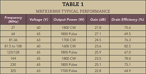
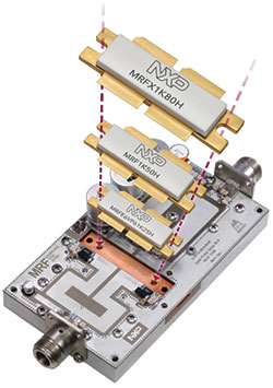
Figure 1 The MRFX1K80H is pin-compatible with existing 50 V LDMOS devices, enabling higher power using the same PCB with little or no retuning.
The first device of the MRFX series was released in August 2017. The MRFX1K80H delivers 1800 W of CW output power and can be used with drain voltages from 30 to 65 V. It has a low thermal resistance of 0.09°C/W and withstands a reflected energy of 65:1 VSWR in all phase angles with no degradation. The typical RF performance at various frequencies is shown in Table 1.
This new transistor demonstrates that raising the drain voltage from 50 to 65 V brings five benefits to RF power amplifier designers. The 65 V drain bias increases the power to 1800 W while retaining a reasonable output impedance. This latter advantage enables a third benefit: the MRFX1K80H was designed to be pin-compatible with existing 50 V LDMOS solutions on the market. As this 1800 W, 65 V transistor has an output impedance close to that of a 1250 W, 50 V transistor, the same PCB can be used (see Figure 1). Little to no retuning is needed, depending on the frequency and the bandwidth, which reduces the development cycle time for faster time-to-market. The fourth benefit is that a higher voltage decreases the current in the system, limiting magnetic radiation and lowering the stress on power supplies and components. Lastly, the new 65 V LDMOS technology exhibits a typical breakdown voltage of 193 V. This higher safety margin improves ruggedness and reliability and enables higher efficiency classes of operation.
NXP warrants production availability of the MRFX1K80H for 15 years. The data sheet, simulation models and other tools may be downloaded from NXP’s website. Reference circuits at various frequencies are available through NXP’s approved distributors.
NXP Semiconductors
Chandler, Ariz.
www.nxp.com/RF