
This W-Band MMIC power amplifier (PA) has a small-signal gain (S21) of 11.2 dB, an input/output reflection coefficient (S11) of −9 dB and saturated output power of 21.4 dBm at 88 GHz. A low loss matching network with power combiner and microstrip coupled lines (MCL) is employed to increase the gain and output power of this three-stage design using WIN Semiconductor’s 0.1 µm GaAs PHEMT process. Compared with metal-insulator-metal (MIM) capacitors, MCLs have greater stability and are less affected by fabrication tolerances. The chip size of the PA is only 2.86 mm ×1.76 mm2.
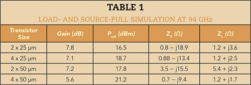
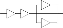
Figure 1 PA design topology.
W-Band (75 to 110 GHz) is largely used for imaging, remote sensing, satellite communications and military and automotive radar. In the automotive market, autonomous cruise control and emergency braking systems employing W-Band transceivers have been developed, but the high cost of mmWave components has widely restricted their use. For these applications, the availability of low cost MMICs is key to market expansion. The development of compact and less expensive W-Band transceiver systems,1 static frequency dividers,2 PAs,3 frequency doublers4 and high gain amplifiers5 have been reported; however, lower cost higher output power (greater than 20 dBm or 100 mW) PAs for linear W-Band systems are still needed.
Recent advances in SiGe and silicon CMOS technologies have demonstrated output power above 100 mW at W-Band,6-8 while compound semiconductors including InP, GaAs and GaN primarily occupy this domain. A narrowband PA using GaAs HEMTs achieved an output power of 25 dBm (316 mW) at 94 GHz,9 while with GaAs MHEMTs, an output power of 213 to 267 mW (23.2 to 24.3 dBm) has been reported.10,11 Several GaAs PHEMT amplifiers have been designed to achieve output powers of 20 to 22 dBm with bandwidths of 10 percent at W-Band.12,13 A two-stage structure was used to deliver 25 dBm at around 94 GHz.14 Over a broad band, a minimum of 14 dBm was obtained, with a peak output power of 16.2 dBm.15
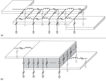
Figure 2 The matching circuit uses a MCL (a) rather than MIM capacitor (b) structure.
Because of their high breakdown voltages and short gate lengths, GaN transistors offer the potential for higher output power at W-Band; however, the results have been limited. Using 0.15 μm gate length GaN transistors, PAs with output powers of 27 dBm at 84 GHz16 and 29 dBm with 15 percent power-added efficiency (PAE) at 88 GHz17 have been reported. Using a 0.12 μm GaN HEMT process on SiC, a three-stage PA has been reported that achieves an output power of 30 dBm, a small-signal gain of 10 dB and PAE of 19 percent at 93.5 GHz.18
In this article, a W-Band GaAs PHEMT MMIC PA with output power above 20 dBm is described. To achieve enough gain in a small chip area, a three-stage topology is employed. The first and second stages are matched to achieve maximum gain. A low loss matching network incorporated with a power splitter (or power combiner) is used in the third stage. The output stage is matched with an impedance determined from load-pull simulation to deliver maximum RF power. Each device is biased class A for high-power gain with high linearity. An overview of the architecture to achieve 21.4 dBm output power is provided. Measured results show good agreement with simulation, demonstrating the capability to meet goals of high performance and low cost for W-Band applications.
CIRCUIT DESIGN
Having sufficiently high ft and fmax, CMOS and SiGe processes are suitable for the fabrication of PAs at W-Band; however, Pout and adequate linearity are important requirements that are better achieved using GaAs processes. Due to the advantages of a semi-insulating substrate and low parasitic inductance of substrate vias, it is also easier to achieve higher levels of mmWave integration.
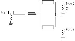
Figure 3 Interstage matching network between stages 2 and 3.
Cell Selection and Topology
As the total gate width increases (more gate fingers and/or wider unit gate width), parasitic effects increase. This reduces available transistor high frequency gain. While the maximum useful device size is different for a given process, generally it is difficult to simultaneously satisfy output power and linearity requirements at W-Band. The GaAs PHEMT process with 0.1 μm gate length is the current industry standard. Maximum practical transistor sizes deliver relatively modest output power. By combining multiple devices, output power can be increased to satisfy a design requirement. Sufficient gain margin is required to compensate additional losses of the combiner networks.
The W-Band amplifier described in this article is based on WIN Semiconductor’s PP10 technology. It is a 0.1 μm GaAs PHEMT process manufactured on 150 mm wafers, with ft > 145 GHz, Fmax > 195 GHz and the capability to operate at 4 V. Measured data of PP10 PHEMT devices was used in the design to ensure the optimization of power and gain while meeting other amplifier requirements.
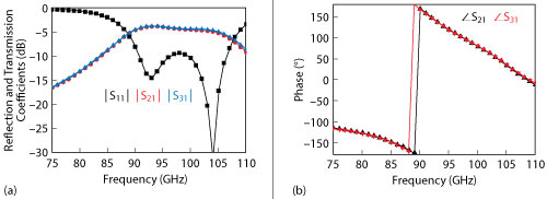
Figure 4 S-parameters of the interstage matching network between stages 2 and 3; magnitude (a) and phase (b).
Small-signal data for a range of different device sizes (unit gate width and number of fingers) was supplied by the foundry. For 2 × 25 and 2 × 50 μm devices, GMAX was greater than 7 dB at 94 GHz. This is higher than can be achieved in a practical circuit, of course, due to interstage and output network losses, matching for optimum power versus gain and the influence of lossy stabilization networks. Published load-pull data indicates that approximately 0.8 W/mm of saturated power density can be achieved with a 4 V bias. The traditional class A bias point at 50 percent Idss (approximately ‐0.4 V Vgs for the PP10-10 process) and 4 V Vds.
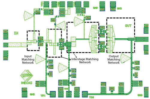
Figure 5 PA layout.
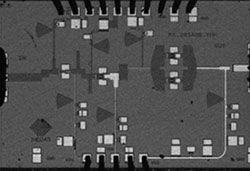
Figure 6 The three-stage amplifier die (2.86 mm × 1.76 mm).
A single transistor PA is first designed for the purpose of device selection. From S-parameters and load- and source-pull simulations, the characteristics of different transistor sizes are obtained, such as small-signal gain, Psat and optimum impedances (see Table 1). In the simulation, all transistors are biased with Vgs = ‐0.4 V and Vds = 4 V. Enlarging the transistor size increases Psat at the cost of reduced gain. Gain also depends more on gate width than on finger number. In this design, both two-finger and four-finger transistors with 50 μm gate widths are used in a three-stage structure to compensate for lower transistor gain.
To achieve sufficient gain, all the transistors are biased class A. The basic topology is shown in Figure 1. A 2 × 50 μm device is used in the first and second stages, and two 4 × 50 μm devices are combined in the third stage. Since each third stage transistor has a saturated output power of 21.2 dBm, two transistors can achieve 24 dBm without considering matching network losses and gain compression from previous stages.
MCL and Matching Network Design
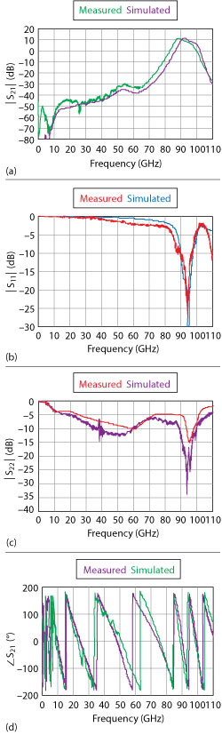
Figure 7 Simulated vs. measured |S21| (a), |S11| (b), |S22| (c) and (c) ∠S21 (d).
For increased stability, the MCL structure is employed for matching and interstage coupling instead of MIM capacitors (see Figure 2). While it is possible to fabricate very small-sized MIM capacitors for this purpose, the losses increase as size is reduced. There are also large variations in capacitance. In the MIM process, a silicon nitride thin film with 150 Å thickness is used as the dielectric material. Silicon nitride has a dielectric constant of 7.5, a resistivity of 1014 Ω cm19 and capacitance per unit area of 0.4 fF/μm2. Variations in dielectric constant, film thickness and area cause corresponding variations in capacitance; deviations of ±10 percent in the MIM capacitors’ properties will severely degrade amplifier performance.
The MCL exhibits less variation because of its very thin effective metal thickness. In general, the gold plating thickness is about 3 mm, while its skin depth is only 0.2 μm at 90 GHz. Even a ±10 percent change in thickness of the plating has little impact on the effective gold metal thickness at mmWave frequencies. Because they are less influenced by process variation, MCLs offer more stable performance.
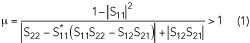
For unconditional stability, the necessary and sufficient condition is μ > 1. Larger values of μ imply greater stability.20,21
Through the use of MCLs in the DC block and matching network, interstage networks and the input and output matching networks, performance variation is reduced and overall stability and yield are improved.
Conjugate impedance matching is employed to achieve high output power. The corresponding source and load impedances ZS and ZL, respectively, are shown in Table 1. The network between stages 2 and 3 is shown in Figure 3, and S-parameters of the test circuit are plotted in Figure 4. The maximum amplitude imbalance is 0.2 dB with a maximum phase difference of 3 degrees. Return loss is better than 10 dB, while insertion loss is only 3.8 dB at 94 GHz.
Bias Network and Stability
High impedance λ/4 shunt stubs are used as bias chokes at the gate and drain ports. W-Band short circuits are realized using large grounding capacitors that are transformed to open circuits through high impedance λ/4 RF paths. DC bias is then applied to the end of the λ/4 line without affecting amplifier performance. W-Band transistors have gain at lower frequencies, as well. It is convenient to use the gate and drain bias networks for low frequency stabilization by introducing resistors and capacitors at the ends of the bias stubs.
The schematic layout of the complete PA including stabilization components is shown in Figure 5. Two cells are directly combined together in a corporate matching network configuration. A cell of the same size is also employed as a driver amplifier. This ensures that the driver stage does not impact power saturation and linearity. To ensure the absence of odd mode and loop oscillation,22,23 further stability analysis is performed.
SIMULATION AND MEASUREMENT
The entire layout was analyzed and optimized using Keysight’s Momentum. Co-simulations were also employed in the schematic environment. The harmonic balance method was used for predicting MMIC PA output power. Figure 6 shows the three-stage amplifier.
The small-signal characteristics were measured with a frequency-expanded HP8510C vector network analyzer. All stages of the PA were biased at Vgs = ‐0.4 V and Vds = 4 V, with the drain currents of the three stages measuring 31.3, 62.5 and 123.4 mA, respectively. The total current was 217.2 mA, and the power consumption was 869 mW.
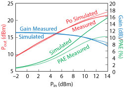
Figure 8 Output power, PAE and gain vs. input power at 88 GHz.
Figure 7 compares the measured and simulated small-signal S-parameters. The maximum measured power gain of the amplifier was 11.2 dB at 88.25 GHz, while the simulated power gain was 11.6 dB at 91.75 GHz. The shapes of the gain and reflection coefficient curves are similar, but the measured passband is shifted lower in frequency by about 3.5 GHz. ∆S21/S21, defined as the relative deviation, is only 3.8 percent. This is attributed to process tolerances and an inadequate simulation of electromagnetic (EM) coupling effects. The MIM capacitor, as previously mentioned, is especially sensitive to process variation. Meanwhile, load/source impedance optimization is sensitive in areas situated around the edges of the Smith chart causing slight process deviations to degrade matching. The measured results show |S11| better than ‐10 dB from 88 to 97 GHz, while S22 is better than ‐10 dB from 89 to 99 GHz.
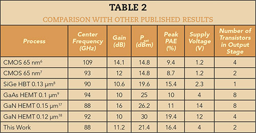
A Keysight E4417A power meter and W8486 power sensor were used to measure output power. A two-port thru-reflect-line (TRL) calibration was performed to shift reference planes to the probe tips. Input power was varied to cover the linear and gain compressed regions. Figure 8 shows output power versus input power at 88 GHz. The amplifier has a linear gain of 11.2 dB and a saturated output power of 21.4 dBm (137.7 mW) at a gain of 7.4 dB. Figure 9 shows output power versus input power at 94 GHz. The amplifier delivers a linear gain of 8.6 dB, saturated output power of 18.2 dBm (66.7 mW) with a gain of 4.7 dB. This amplifier is compared with previously published results using different process technologies in Table 2.
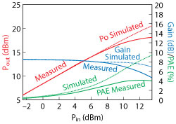
Figure 9 Output power, PAE and gain vs. input power at 94 GHz.
CONCLUSION
A W-Band PA is designed and fabricated using WIN Semiconductor’s 0.10 µm GaAs PHEMT process. MCLs are used for matching to flatten the gain response and decrease matching network sensitivity to the fabrication process. The three-stage MMIC PA achieves a gain of 11.2 dB and a saturated output power greater than 21.4 dBm at 88 GHz. The die size is 2.86 mm x 1.76 mm2. Simulated performance is in good agreement measurements.n
ACKNOWLEDGMENTS
This work is supported by the Major Program of the National Natural Science Foundation of China (Grant No. 61434006) and the National Natural Science Foundation of China (Grant No. 61401457 ). The authors would also like to acknowledge WIN Semiconductors for development of the PHEMT MMIC process used for the PA.
References
- P. Kangaslahti, T. Gaier, D. Dawson, J. Tuovinen, T. Karttaavi, M. Lahdes et al., “Low Noise Amplifiers in InP Technology for Pseudo Correlating Millimeter Wave Radiometer,” IEEE MTT-S International Microwave Symposium Digest, May 2001, pp. 1959-1962.
- Z. Youtao, L. Xiaopeng, Z. Min, C. Wei and C. Xinyu, “A 83 GHz InP DHBT Static Frequency Divider,” Journal of Semiconductors, April 2014, Vol. 35, No. 4, pg. 045004.
- Y. Hongfei, C. Yuxiong, W. Danyu, N. Xiaoxi, S. Yongbo and J. Zhi, “A 16.9 dBm InP DHBT W-Band Power Amplifier with More Than 20 dB Gain,” Journal of Semiconductors, July 2013, Vol. 34, No. 7, pg. 075005.
- Y. Hongfei, W. Xiantai, W. Danyu, S. Yongbo, C. Yuxiong, G. Ji, N. Xiaoxi and J. Zhi, “W-Band Push–Push Monolithic Frequency Doubler in 1-um InP DHBT Technology,” Journal of Semiconductors, March 2013, pg. 095006.
- Z. Yinghui, Z. Yuming, Z. Yimen, C. Yuxiong, Y. Hongfei, W. Xiantai, L. Hongliang, L. Xinyu and J. Zhi, “A W-Band Two-Stage Cascode Amplifier with Gain of 25.7 dB,” Journal of Semiconductors, Vol. 34, No. 12, December 2013, 34(12), pp. 125003-1-5.
- Q. J. Gu, Z. Xu and M. C. F. Chang, “Two-Way Current-Combining W-Band Power Amplifier in 65-nm CMOS,” IEEE Transactions on Microwave Theory and Techniques, Vol. 60, No. 5, May 2012, pp. 1365-1374.
- K. J. Tsai, J. L. Kuo and H. Wang, “A W-Band Power Amplifier in 65-nm CMOS with 27 GHz Bandwidth and 14.8 dBm Saturated Output Power,” Radio Frequency Integrated Circuits Symposium, June 2012, pp. 69-72.
- M. Chang and G. M. Rabeiz, “A Wideband High-Efficiency 79–97 GHz SiGe Linear Power Amplifier with >> 90 mW Output” Bipolar/BiCMOS Circuits and Technology Meeting, November 2008, pp. 69-72.
- V. Dyadyuk, J. Kendall, J. Pathikulangara, O. Sevimli and L. Stokes, “Improved Spectral Efficiency for a Multi-Gigabit MM-Wave Communication System,” European Microwave Conference, October 2007, pp. 810-813.
- A. Tessmann, A. Leuther, C. Schwoerer and H. Massler, “Metamorphic 94 GHz Power Amplifier MMICs,” IEEE MTT-S International Microwave Symposium Digest, June 2005, pp. 1579-1582.
- K. J. Herrick, K. W. Brown, F. A. Rose, C. S. Whelan, J. Kotce, J. R. Laroche and Y. Zhang, “W-Band Metamorphic HEMT with 267 mW Output Power,” IEEE MTT-S International Microwave Symposium Digest, Vol. 2, June 2005, pp. 843-846.
- H. Y. Chang, H. Wang, M. Yu and Y. Shu, “A 77 GHz MMIC Power Amplifier for Automotive Radar Applications,” IEEE Microwave Guided Wave Letters, Vol. 13, No. 4, April 2003, pp. 143-145.
- APH635 Datasheet, Northrop Grumman Corp, 2011, www.as.northropgrumman.com/products/APH635rev12.11.pdf.
- P. Huang, E. Lin, R. Lai, M. Biedenbender, T. W. Huang, C. Geiger, T. Block and P. H. Liu, “A 94 GHz Monolithic High Output Power Amplifier,” IEEE MTT-S International Microwave Symposium Digest, June 1997, pp. 1175-1178.
- B. Kim, A. Tran and J. Schellenberg, “Full W-Band Power Amplifier/Combiner Utilizing GaAs Technology,” IEEE MTT-S International Microwave Symposium Digest, June 2012.
- M. Micovic, A. Kurdoghlian, H. P. Moyer et al., “GaN MMIC PAs for E-Band (71 GHz–95 GHz) Radio,” IEEE Compound Semiconductor Integrated Circuits Symposium, October 2008.
- M. Micovic, A. Kurdoghlian, K. Shinohara et al., “W-Band GaN MMIC with 842 mW Output Power at 88 GHz,” IEEE MTT-S International. Microwave Symposium Digest, May 2010.
- M. Micovic, A. Kurdoghlian, A. Margomenos et al., “92–96 GHz GaN Power Amplifiers,” IEEE MTT-S International Microwave Symposium Digest, June 2012.
- S. M. Sze, Physics of Semiconductor Devices, John Wiley & Sons, 1981.
- D. M. Pozar, Microwave Engineering, 2nd Edition, Wiley, N.Y., 1998.
- M. L. Edwards and J. H. Sinsky, “A New Criterion for Linear 2-Port Stability Using a Single Geometrically Derived Parameter,” IEEE Transactions on Microwave Theory and Techniques, Vol. 40, No. 12, August 1992, pp. 2303-2311.
- M. Jankowski, E. Limiti and P. E. Longhi, “Freitag Method Application to PA Stability Test,” IEEE Workshop on Integrated Nonlinear Microwave and Millimeter-Wave Circuits, 2008, pp. 149-152.
- M. Ohtomo, “Stability Analysis and Numerical Simulation of Multidevice Amplifiers,” IEEE Transactions on Microwave Theory and Techniques, Vol. 41, No. 6, July 1993, pp. 983-991.