
The next digital transformation is rapidly approaching with evolving technologies in 5G, the internet of things (IoT), artificial intelligence (AI) and Industry 4.0 automation. These radio frequency (RF) technologies will take us into the next cultural step change with driverless cars, smart cities, machine to machine connectivity, healthcare wearables, and disruptive innovations in 3D technology.
The explosion in these disruptive technologies has created a surge in demand for advanced semiconductors. The Wall Street Journal recently noted:
“Semiconductors are in nearly every electronic gadget and home appliance. In 2014, there were 3.8 billion connected “things” world-wide, from televisions to baby monitors to thermostats, according to Gartner Inc., which projects that number will rise to 8.4 billion this year and 20.4 billion by 2020. Analysts estimate revenue from chips will double, if not triple, in the next decade.” – Wall Street Journal, 4/26/2017
Consequently, the semiconductor industry has seen massive consolidations, unprecedented R&D spending, and a race innovation among the industry’s top players. Devices enabling this next transition from “Big Data” to ”Massive Data” are designed for phased array beam steering, spatial multiplexing, massive multiple-input and multiple-output (MIMO), and air interfaces. They are also pure indicators of another round of explosive data growth.
The Opportunity
The manufacturing of these RF devices that will drive the technology of tomorrow is extremely complicated, generated from an abundance of complex wafer processes and designed from a vast array of components creating full systems on a chip (SOC). Consequently, the amount of data generated from manufacturers has grown exponentially – from device design through final package test. The data is structured, unstructured, complex, and requires computational mathematics, conversions and alignment to the business; it is not uncommon to see over one billion data points a week just from production test equipment. Many fabs see the management of this data as their greatest burden when in reality it could be their greatest asset. Their productivity could improve dramatically through appropriately leveraging the data. How? To begin with, a sophisticated data initiative requires the appropriate level of support and corporate structure.
Designing Corporate Structure for Advanced Data Analytics
The preponderance of fabs today fail to fully leverage their data capabilities because of their corporate structure. Typically, the data analytics' function reports through information technology (IT) or within manufacturing, presenting two problems. First, data analysis and technology are fundamentally different functions. IT managers often lack an understanding of big data analytics, and therefore fail to fully utilize the opportunities data presents. Second, and most critically, data analytics risks being siloed. Having data engineers report through IT limits their opportunities to work cross-functionally. Sophisticated data analysis will benefit and build coordination across every functional group within a fab. To fully optimize the potential benefits of a company’s data, data management and analysis must be conducted cross-functionally – subordinating data analytics within any particular function stands to severely limit the benefits it could provide.
A successful advanced analytical initiative requires a strategic corporate vision that needs deliberate support and prioritization from the top down, and an autonomous, stand-alone corporate business group dedicated solely to data. Corporate executives must enable this group to incorporate and synchronize core business systems, design centers, wafer fabrication locations and production manufacturing factories. This effort will create a company-wide system that promotes cross-functional collaboration through seamless digital communication, production synergy and business intelligence. The question then becomes: who belongs on this team, and how should it be structured?
Building a Data Analytics Team
Big data analytics tools are extremely complex and programming-intensive. Perspective analytic design, machine learning, automation and artificial intelligence require a variety of skills. It is essential that this endeavor be managed by those with the proper core competencies capable of fully supporting the design development demands of the future. An ideal Data Analytics Group is illustrated in Figure 1.
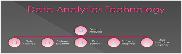
Key team members and skill sets:
- Director – Reports to Chief Engineering Officer or Chief Technical Officer
- Data Architect – Provides technical and system-wide insight
- Data Scientist – Designs complex algorithms, applied statistics, cognitive science
- Systems Engineer – Extraction expert, integration, translation & distributive computing
- Software Engineer – Designs database, advanced programming languages, web services
- User Interface Designer – Builds intuitive and streamlined user interface for tools
Creating Cross-Functional Data Alignment
The primary function of the Data Analytics Group is identifying and organizing the data being generated by the manufacturer; then creating a framework through which the flow of data can be structured and managed.
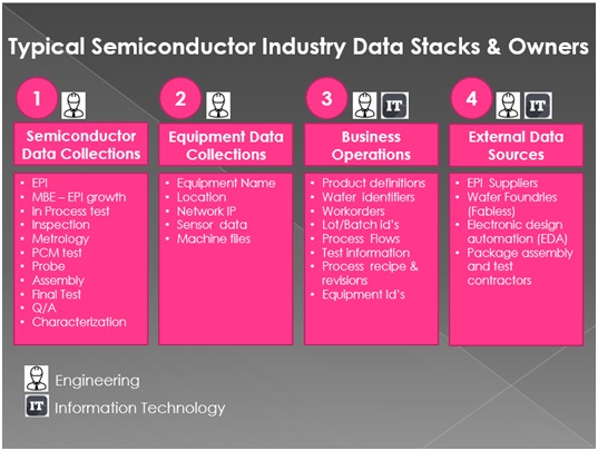
Figure 2 illustrates a framework using four stacks to demonstrate the data generated in manufacturing. The first two stacks support wafer fabrication through manufacturing and contain layers of raw data generated from test, process and capital equipment. Data stack three contains business execution properties that house work orders, lot numbers, product identifiers, processes and workflows. Data stack four supports external data sources.
The Data Analytics Group works with each business unit to identify the disparate sources of data and establish what is most important to the company. Once the data silos and processes are identified, each is thoroughly examined and documented for ownership, structure, data content, formats and existence of business enterprise data. The importance of enterprise metadata is crucial for successful analytics as it provides alignment between the business processes, and the data collections. Data relationships formed are used in designing connected layers that will provide insight for yield improvement, productivity, equipment optimization, performance and actionable decision making.
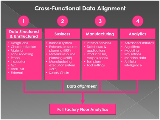
The product of this initiative is cross-functional data alignment. Figure 3 demonstrates the data alignment requirements across business functions. The alignment defines the exact data relationships tied to business operations, manufacturing processes, internal rules, databases, algorithms or product specific applications. The alignment provides full genealogy to the unstructured data and provides levels of manufacturing intelligence for the analytics team.
The data silos contain raw data that is often in multiple formats. These files will need to be transformed and combined for analytical intent. Software tools must be designed to provide real time extraction, translation and loading (ETL) of raw data files into scientific information. Database relationships are derived with the required business enterprise extracts. These associations provide connectivity and genealogy to fab processes, work orders, production and external sources.
Once the design framework is reviewed and communicated, the initial design of analytics can begin, providing insight to operational efficiencies, continuous yield improvements, failure analysis, process optimization and general statistics. Advanced analytics is a continuous process that will change with business developments, but a sound architecture provides purposeful, accurate and timely data for the entire corporation.
Driving Manufacturing with Advanced Data Analytics
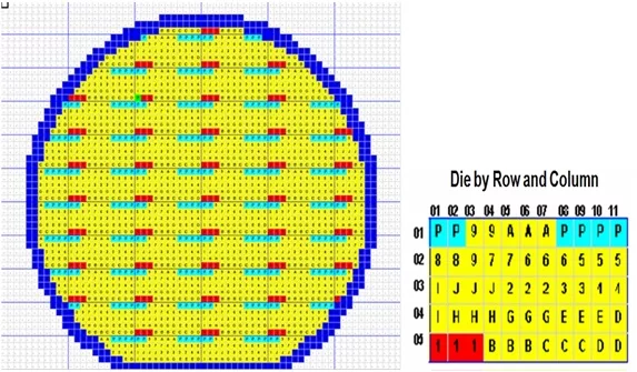
Once data alignment framework is established, analytics can be used to create a digital die definition footprint that can be used in a multitude of processes to streamline manufacturing.
Precise die definition for each wafer design, as shown in Figure 4, is the distinctive physical footprint necessary for visual analytics, internal application design, and integration with 3rd party software. These digital definition files are easily translated and converted. The digital files are then to be used throughout fab and fabless manufacturing operations for known good die (KGD) strategies, controlling die movements on capital, machine optimization schemes, upstream manufacturing and cognitive analytics.
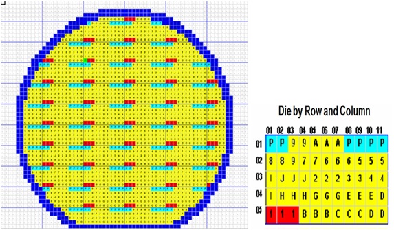
The wafer map definition originates at design layout and is extracted through GDS files. Translation routines are used to convert this information into digital wafer maps, containing specific die definition, test structures and process control monitors. The maps can also be used to generate various machine files. Throughout the manufacturing process, precise die definition is recorded in all data collections.
Production can leverage the digital die definition to drive each of the following sequential steps in semiconductor manufacturing:
1. Efficiencies at wafer probe die sort and machine files:
In wafer probe operations, digital wafer maps are manipulated creating specific probing profiles to optimize capital. This capability provides sample probe patterns used for high yielding components, identifies non-probe edge exclusions zones and can be used for creating post-probe maps that allow for the re-test of only the failing die.
These methods can provide capital efficiencies of up to 11.5–18.0% based on product mix just by implementing probing efficiency.
 2. Die Inspection
At the die inspection process, digital map results from wafer probing are converted into machine inspection files. These wafer-specific files control the machine movements, examining only those with passing wafer probe results for visual defects. Wafer throughput can improve by up to 12-14% at die inspection based on mix.
In most large-scale semiconductor manufacturers today, these efficiencies would equate to millions of dollars per year in savings.
3. Off-Line Data Processing
Consideration should be given to the benefits of processing data results at a central location off line from fabrication and manufacturing tools. In this off-line model, software and services allow wafers to be screened to multiple limit sets, to calculate initial statistics, to automate wafer dispositioning processes and to create upstream machine files for inspection and die attach. A major cost savings with this model is its ability to re-screen wafers without the need for retest. Wafers in inventory or in need of disposition can be released to production with new die attach map files from re-screened product.
4. Incorporation of Software and Tools
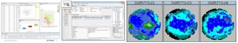
There are some powerful third party software tools from companies like Optimal+ and National Instrument’s DIAdem that can greatly assist with central data collection efforts. These packages often support integration with other databases and contain a number of visual analysis tools for the end user. A sample of the output is provided in Figure 5.
6. Web Services
Web service portal designs, as shown in Figure 6, allow for optimization of manufacturing tools, delivering real-time visual analytics on interactive dash boards of manufacturing performance indicators, KPI metrics, equipment efficiencies (OEE) and applications for full data genealogy extractions.

Today, best-in-class manufacturers leverage advanced data analytics in their production process. Manufacturers hoping to stay competitive must do the same. However, while data analytics is critical in improving manufacturing, it’s most important impact is in design engineering. A semiconductor manufacturer’s success in the manufacturing industry from hereon will be determined by the extent to which it leverages advanced data and artificial intelligence in design engineering and verification.
Data-Driven Design Engineering and Verification
Product-market lead time has increased proportionally with each node of functionality. As circuit designs become increasingly complicated, so too does the design verification process, with an enormous volume of data, necessary for predictive analytics, device analysis and machine learning algorithms. Design engineering labs filled with expensive RF testing equipment are continuously pumping out massive files used in validating design performance across the RF communication spectrums. When one also considers the thousands of mathematical modelling computations, design simulations, reliability requirements, characterization, system software and final test needs, it is surprising that engineering staffs can produce devices in a 12-18 month timeframe.
To address these design demands, manufacturers must begin to invest heavily in engineering talent. Today, their efforts are far from adequate. Most of this device analysis today is still seen as a function within design engineering. This needs a fundamental change in the semiconductor industry, where engineers are unjustifiably scarce. In the U.S., there are presently over 5,000 open positions on LinkedIn looking for talented engineers in areas of design or verification. A recent study conducted by the Manpower Group concluded:
“Engineers have appeared on the list of hardest to fill jobs in the U.S. for the past nine years; globally, engineers are the fourth most difficult to fill position. Competition for top engineering talent continues to challenge employers, requiring them to re-examine attraction and retention strategies.” – ManpowerGroup1
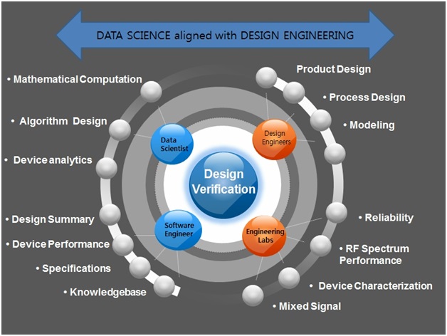
As modeled in Figure 7, the deep technical skill sets of software engineers and data scientists align perfectly with device design engineering teams. Experts in data science and software engineering can collaborate to advance design verifications methods by providing rapid design insight through the deployment of device algorithms, predictive analytics, and machine-learning tools. This insight will provide engineering staff with a deeper understanding of their designs by providing them with device-specific analytics in overall performance, reliability, and fault tolerance. Beyond adding value by improving the immediate design verification methods, the algorithms built will develop their own substantial intrinsic value, and will prove to be invaluable assets to the entire design operation.
1 “2016/2017 U.S. Talent Shortage Survey,” ManpowerGroup, http://www.manpowergroup.us/campaigns/talent-shortage/assets/pdf/2016-Talent-Shortage-Whitepaper.pdf
Data Software Intellectual Property
Internal IP software developments from this partnership can form significant competitive advantages. Below, several examples of where manufacturers can benefit is provided.
Example 1. Advanced Prototyping
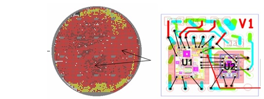
Advanced prototyping methodologies are one example demonstrating the value of internally developed manufacturing IP. Advanced prototyping involves deep die parametric searches, surveying wafers to locate specific devices used for design builds. In Figure 8, these algorithms search through wafer lots locating actual die as determined from model simulations and used for prototype builds testing design centering, corner builds and device stack-up tolerances.
Example 2. Advanced Analysis Software
Specific software tools developed for mathematical computations and algorithm design needs, combined with scientific products used for modelling and simulation like those from Mathworks, as shown in Figure 9, can assist in developing best-in-class advanced analytics used for product development, R&D, design, verification and machine-learning.

Benefits Model
The model in Figure 10 is a break-out of the cognitive benefits delivered by a centralized data science organization, creating an environment of analytical discovery. The specific tools crafted for each organization support world-class manufacturing standards with methodologies targeting key performance metrics, manufacturing optimization and end-to-end line yields providing complete corporate visibility from a suite of scientific tools.
In manufacturing, data science analytics provide cost-saving initiatives through the distribution of real-time corporate intelligence used for proactive process improvements, expediting yield analysis, insight to overall equipment efficiencies (OEE), active work-in-process (WIP) management, return on invested capital (ROIC), resource management, and prioritizing quality improvement efforts.
The most significant and most complicated benefit will come from specific internal product design efforts with an IP knowledgebase produced from automated data acquisitions, number crunching, learned artificial intelligence and distributed analysis reporting used for R&D, device design, and product verification activities. This IP has compound benefits from maximizing engineering resources, reduced time to market with custom analytical tools that nurture an environment of engineering discovery, to a new team of data scientists who understand their needs and speak their language.

Summary
As demand for device functionality increases so does product development complexity, productivity costs, resource allocation and time-to-market. These are all best addressed with big data solutions. The need for robust data science technology organizations in the semiconductor industry cannot be overstated. This is no longer a luxury; it is a necessity. Those investing in the science of data technology may just determine what companies successfully advance in the industry.