
A 76 to 77 GHz GMIC Mixer for
Automotive Radar
A 76 to 77 GHz mixer that uses flipped Hewlett-Packard HSCH-9401 Schottky diodes has been developed on a 127-µm-thick glass microwave integrated circuit (GMIC) for autonomous cruise control (ACC) radar applications. The design process for diode modeling and mixer development is presented. A 6 dB average conversion loss is measured with an LO input power level of 8 to 15 dBm at room temperature. Measured mixer results produced excellent agreement with theory.
Thomas P. Budka, David Antopolsky and Matthew T. Pizzella
M/A-COM, Lowell, MA
A balanced mixer uses a hybrid junction (90° or 180°) along with two single-ended mixers to provide better return loss at all inputs as well as better RF/LO isolation.1 Another added benefit of a balanced mixer is AM noise cancellation from the LO.1 In the ACC application, a rat race coupler is selected for the hybrid junction along with two flipped Schottky diodes on a 127-µm-thick GMIC. This article presents the diode modeling and mixer design approach along with the measured results of the 76 to 77 GHz mixer.
 Diode Model Development
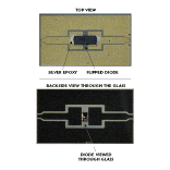
Diode models of the HSCH-9401 device were developed before starting this mixer design. A 50 W series coplanar waveguide (CPW) test fixture was fabricated on thick glass. First, a passive model for the CPW structure was derived based on measurements. Next, five HSCH-9401 Schottky diodes were flip-chip mounted to test sites using silver epoxy and RF tested over a wide range of bias voltages (-4, -2, 0, 0.3, 0.6, 0.73 and 0.78 V) up to 40 GHz. Figure 1 shows top and backside views of a flipped diode on the test fixture. Figure 2 shows the measured vs. modeled data at four forward bias voltages. The diode model is first fit at V = 0.3 V. Next, the bias on the model is changed to 0.6 V to 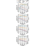 determine if the model is valid for the V = 0.6 V S parameters. The diode parameters were then changed so that the model fit both the 0.6 and 0.3 V data. Because the diode is highly nonlinear above the knee voltage, it becomes increasingly difficult to fit a model at the higher bias voltages such as 0.73 and 0.78 V. Additional iterations proved successful in fitting the diode model at all four bias voltages. The iterations were stopped at 0.78 V because the additional modeling became time prohibitive.
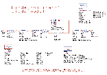 Figure 3 shows the flipped diode model on a 127-µm-thick GMIC based on the measurements up to 40 GHz. (Pad models have been modified for a microstrip environment. Length dimensions are in mils.) The CPW feeds have been replaced with an equivalent GaAs-covered microstrip feed. Two-dimensional modeling produced an equivalent microstrip substrate -- GaAsonGlass -- with a dielectric constant of 8 for the GaAs pads of the flipped diode on GMIC.
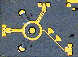 Figure 4 shows the top view of the 76 to 77 GHz GMIC mixer fabricated on 127-µm-thick glass. First, a low value series capacitor is designed for the RF and LO inputs. Video leakage from a radar system can be minimized by keeping the series capacitance low. A three-finger interdigital capacitor is used. Next, the rat race coupler is designed and optimized for good LO/RF isolation. All tee junctions were modeled using HP Momentum electromagnetic simulation software and then fitted to an equivalent linear circuit model. It is extremely important to fit an equivalent linear circuit model to each element because harmonic balance analysis requires S parameters at many higher harmonics. It was determined that HP Momentum and Sonnet EM simulators become unstable above 200 GHz and produce unphysical results for 127-µm-thick GMIC.
The IF output is designed to be a 10 GHz maximally flat lowpass filter. Next, all the elements were combined to create the mixer schematic. The line lengths to the diode from the coupler ring were optimized along with the line length after the diode to the via to provide the best conversion loss. Once an optimal single design was achieved, Monte Carlo yield analysis was used to further improve the design. Both diode variations and chip placement variations were included. Monte Carlo analysis predicts a 90 percent yield for a conversion loss of less than 6 dB from 74 to 78 GHz.
During electromagnetic simulations of the interdigital capacitor structure, radiation was discovered at approximately 70 GHz. Additional detailed modeling showed that this radiation suckout could be pushed to a lower frequency with the extension of a slot at the tip of the center finger. Users of interdigital capacitors of three fingers or more are cautioned to trust the results of electromagnetic simulations when suckouts are observed. This suckout was observed in measurements of both a scale model at 3 GHz and the actual GMIC structure at 70 GHz.
 Measurements
Waveguide RF probes are used at the RF and LO ports while a lower frequency probe is used to extract the IF. Figure 5 shows the measured and modeled conversion loss of this mixer at 76.6 GHz with an RF input level of -9.4 dBm. There is surprisingly good agreement between the measured and original modeled conversion loss of 6 dB with an LO input drive level from 8 to 15 dBm.
Conclusion
This article described the modeled and measured results of a 76 to 77 GHz mixer. The diode model for a flipped HSCH-9401 Schottky diode was presented and compared with measured results up to 40 GHz. This model was then used successfully to design a 76 to 77 GHz mixer, thereby demonstrating the validity of the extrapolated diode model at 76 GHz. The mixer provided 6 dB conversion loss at 76 GHz for an LO power level of 8 to 15 dBm as predicted by the mixer model.
Acknowledgment
The authors would like to thank Nitin Jain, Peter Staecker, Angelos Alexanian, Dan Swanson, Dennis Wells, Allan Douglas, Noyan Kinayman and Brian Lester for technical discussions during this design.
Reference
1. D.M. Pozar, Microwave Engineering , Addison-Wesley Publishing Co., 1990.
Thomas P. Budka received his AB degree in physics from Dartmouth College, Hanover, NH in 1989 and his MA degree in physics from The University of Rochester, Rochester, NY in 1991. He received his PhD degree in electrical engineering from The University of Michigan’s department of electrical engineering and computer science in Ann Arbor, MI in 1995. From 1995 to 1998, Budka worked as a MMIC designer at Texas Instruments/Raytheon TI Systems developing flip-chip embedded transmission line MMIC power amplifiers. From 1998 to 1999, he worked for M/A-COM’s Research and Development group designing/developing a low cost 76 GHz radar system on a single chip. Presently, Budka is a staff RF design engineer with RF Micro Devices’ Boston Design Center focusing on advanced product development. He is also a member of the IEEE Microwave Theory and Techniques Society.
David M. Antopolsky received his BS and MS degrees in electrical engineering from the Georgia Institute of Technology, Atlanta in 1996 and 1998, respectively. In 1997, he worked as an intern at Texas Instruments/Raytheon TI Systems. While in graduate school he was a teaching assistant and research assistant. Antopolsky is currently working at M/A-COM’s Corporate Research and Development group as a senior engineer. His research interests include RF/microwave circuit design and test. Antopolsky is a member of Eta Kappa Nu and Tau Beta Pi.
Matthew Pizzella received his BSEE from Pennsylvania State University in 1996. From 1996 to 1999, he worked at M/A-COM’s Corporate Research and Development group where he was involved in transistor development, characterization and modeling. Pizzella is presently employed with Philips Broadband as an RF design engineer.